China Extreme Ultraviolet (EUV) Lithography Market Size, Share & Forecast 2026–2034
Report Highlights
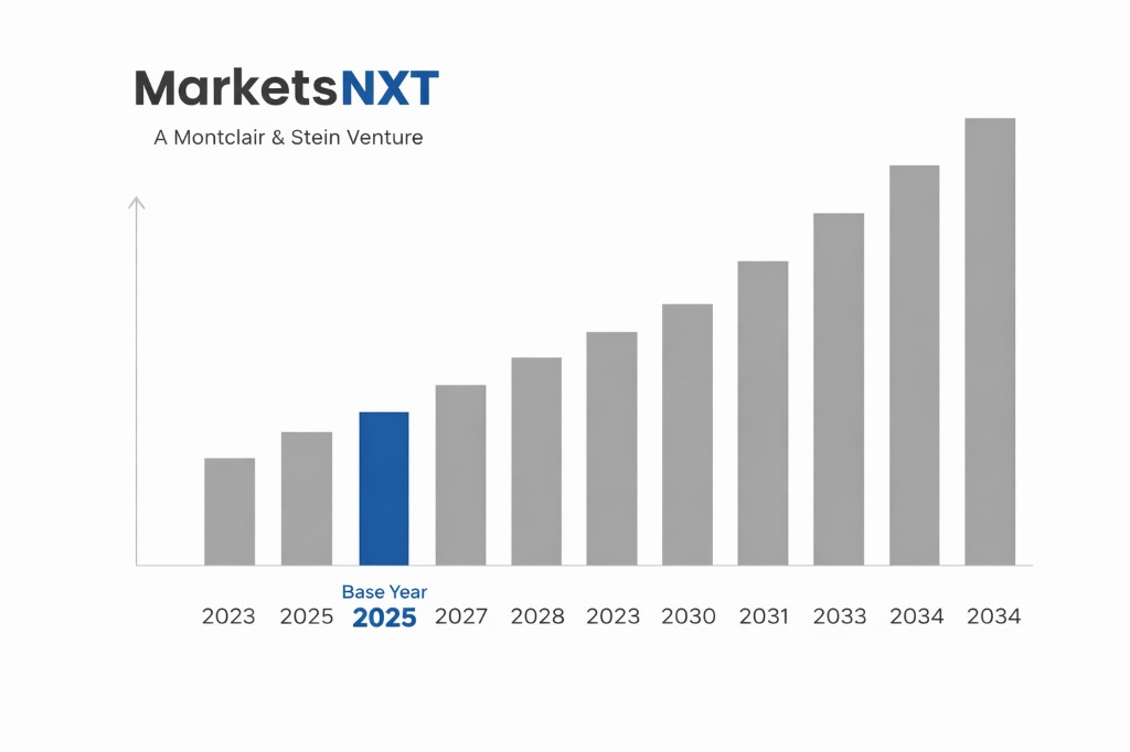
- ✓Market Size 2024: USD 247 million
- ✓Market Size 2032: USD 892 million
- ✓CAGR: 17.4%
- ✓Market Definition: Extreme ultraviolet lithography systems and related components used in advanced semiconductor manufacturing for nodes below 7nm. Includes EUV scanners, photomasks, photoresists, and metrology equipment.
- ✓Leading Companies: ASML, SMIC, ChangXin Memory Technologies, Hua Hong Semiconductor, Advanced Semiconductor Engineering
- ✓Base Year: 2025
- ✓Forecast Period: 2026-2032
Analyst Recommendation — Domestic Hedging Strategy: Equipment suppliers should establish joint ventures with Chinese partners before 2026 to secure market access ahead of potential export control expansions while Beijing prioritizes self-sufficiency in semiconductor manufacturing equipment.
Extreme Ultraviolet Lithography in China: Market Overview
China's extreme ultraviolet lithography market represents a critical battleground in global semiconductor competition, valued at USD 247 million in 2024 despite significant technology transfer restrictions. The market structure reflects heavy government intervention through the National IC Fund and state-owned enterprises, with SMIC leading domestic foundry development and memory manufacturers like ChangXin Memory Technologies driving advanced node requirements. Policy initiatives under the 14th Five-Year Plan have designated EUV technology as a strategic priority, creating a market dynamic where government procurement decisions outweigh traditional commercial considerations in equipment acquisition and deployment strategies.
The current market architecture demonstrates how geopolitical tensions have fundamentally altered technology adoption patterns, with Chinese companies forced to develop workaround solutions while simultaneously investing in indigenous EUV research capabilities. ASML's restricted access to Chinese customers has created supply bottlenecks that paradoxically strengthen domestic equipment manufacturers like Naura Technology and Advanced Micro-Fabrication Equipment, though these companies remain several generations behind in EUV capabilities. The market's growth trajectory depends heavily on Beijing's ability to navigate export controls while building comprehensive semiconductor manufacturing ecosystems that can support advanced lithography requirements without foreign dependency.
Policy-Driven Growth in the Chinese EUV Market
The National Integrated Circuit Industry Development Guidelines, implemented through the Ministry of Industry and Information Technology, provides direct subsidies totaling USD 12.8 billion specifically for advanced lithography equipment acquisition and development. The National IC Fund's Phase III capital injection of USD 47 billion includes dedicated allocations for EUV technology transfer partnerships and indigenous research programs, with SMIC receiving USD 2.3 billion in direct funding for 7nm and 5nm production line establishment. These policy mechanisms translate into guaranteed purchase orders for EUV systems, creating artificial demand that supports market growth despite technical and supply chain limitations imposed by international restrictions.
The Made in China 2025 initiative establishes specific procurement mandates requiring 70% domestic content in semiconductor manufacturing equipment by 2030, driving forced localization in EUV supply chains. Regional governments in Shanghai, Shenzhen, and Hefei provide additional tax incentives worth up to 50% of equipment costs for companies investing in advanced lithography capabilities, with compliance timelines requiring full implementation by December 2027. The China National Nuclear Corporation's laser technology development program, allocated USD 890 million under the National Medium and Long-term Program for Science and Technology Development, specifically targets EUV light source indigenization to reduce dependence on foreign suppliers like Cymer and Gigaphoton.
Regulatory Barriers and Compliance Costs
The Ministry of Commerce's Catalogue for the Guidance of Foreign Investment Industries restricts foreign ownership in semiconductor equipment manufacturing to minority stakes, requiring complex joint venture structures that delay market entry by 18-24 months. The Cybersecurity Law mandates data localization for all EUV system operational data, imposing compliance costs of USD 15-25 million per manufacturing facility for secure data infrastructure development. The National Development and Reform Commission requires environmental impact assessments for EUV installations, with approval timelines extending 6-8 months and additional costs of USD 2-4 million per site for specialized clean room certifications and electromagnetic shielding compliance.
Export control compliance creates additional regulatory burden, with the State Administration for Market Regulation requiring detailed technology transfer documentation and approval processes that can extend equipment delivery timelines by 12-18 months. The Ministry of Finance's import duty structure imposes 25% tariffs on certain EUV components not manufactured domestically, while providing exemptions for equipment meeting specific technology transfer requirements, creating a complex cost calculation that varies significantly based on procurement strategy. The China Securities Regulatory Commission requires public disclosure of all foreign technology dependencies for listed semiconductor companies, imposing transparency costs and potential market valuation penalties for companies relying heavily on imported EUV systems.
Policy-Created Opportunities in China
The National Smart Manufacturing Development Plan creates specific procurement opportunities for EUV-enabled production lines, with the Ministry of Industry and Information Technology allocating USD 3.2 billion in direct contracts for domestic foundries upgrading to advanced node capabilities. The Greater Bay Area Development Plan establishes dedicated EUV research corridors in Shenzhen and Guangzhou, providing land use rights, tax exemptions, and infrastructure subsidies worth USD 850 million for companies establishing EUV-related manufacturing and research facilities. Beijing's National Laboratory for Extreme Manufacturing initiative offers joint research contracts worth USD 420 million specifically for EUV technology development partnerships between foreign equipment suppliers and domestic research institutions.
The Central Government's Strategic Emerging Industries Development Fund creates guaranteed financing mechanisms for EUV equipment purchases, with the China Development Bank providing preferential loan rates of 2.5% below market rate for approved lithography projects. Provincial governments in Jiangsu and Zhejiang offer additional incentives including 15-year property tax exemptions and utility cost subsidies for EUV manufacturing facilities, with combined value reaching USD 45-60 million per major installation. The National Innovation Demonstration Zone program grants fast-track approval processes for EUV technology imports meeting specific indigenization requirements, reducing regulatory compliance timelines from 18 months to 6 months for qualifying projects.
Market at a Glance
| Metric | Value |
|---|---|
| Market Size 2024 | USD 247 million |
| Market Size 2032 | USD 892 million |
| Growth Rate (CAGR) | 17.4% |
| Most Critical Decision Factor | Export control compliance and technology transfer restrictions |
| Largest Region | Yangtze River Delta |
| Competitive Structure | Foreign-dominated with restricted access and emerging domestic players |
Leading Market Participants
- ASML Holding
- Semiconductor Manufacturing International Corporation (SMIC)
- ChangXin Memory Technologies
- Hua Hong Semiconductor
- Advanced Semiconductor Engineering
- Naura Technology Group
- Advanced Micro-Fabrication Equipment (AMEC)
- Shenzhen Microelectronics Technology
- Beijing E-Town Semiconductor Technology
- China Resources Microelectronics
Regulatory and Policy Environment
The Semiconductor Industry Development Regulations, administered by the Ministry of Industry and Information Technology under State Council Decree No. 729, establish the primary legal framework governing EUV technology acquisition and deployment in China. The National Development and Reform Commission oversees foreign investment approvals through the Foreign Investment Law implementation guidelines, requiring technology transfer commitments and domestic partnership structures for EUV equipment imports exceeding USD 50 million. Key compliance requirements include mandatory data localization under the Cybersecurity Law, technology security reviews administered by the Cyberspace Administration of China, and export control compliance verification through the Ministry of Commerce, with penalties including equipment seizure and operational license revocation for non-compliance.
Upcoming regulatory changes include the proposed National Semiconductor Equipment Security Review Regulation, expected implementation in Q3 2026, which will require pre-approval for all EUV system installations and mandate domestic alternative development timelines. The draft Foreign Investment Security Review Measures will expand government authority to block or unwind EUV technology acquisitions deemed threatening to national security, with retroactive application to transactions completed after January 2025. Compared to regional frameworks, China's approach emphasizes technology indigenization and supply chain security more aggressively than South Korea's market-based incentives or Taiwan's industry-led development model, creating a unique regulatory environment that prioritizes strategic autonomy over immediate commercial efficiency in EUV technology adoption.
Long-Term Policy Outlook for Chinese EUV Market
By 2032, China's semiconductor self-sufficiency goals under the National Strategy for Integrated Circuit Development will likely result in comprehensive domestic EUV capabilities, supported by USD 150 billion in cumulative government investment through the National IC Fund phases and provincial co-investment programs. The 15th Five-Year Plan, covering 2026-2030, is expected to establish mandatory domestic content requirements reaching 80% for semiconductor manufacturing equipment, effectively excluding foreign EUV suppliers from new installations unless they establish substantial technology transfer and local production commitments. Policy emphasis will shift from equipment acquisition to ecosystem development, with the Ministry of Science and Technology's National Laboratory system targeting breakthrough achievements in EUV light sources, photoresists, and precision optics through coordinated research programs.
The anticipated China-Europe Semiconductor Cooperation Agreement, under negotiation for 2027 implementation, may create limited channels for continued EUV technology access in exchange for market access commitments and joint research initiatives. However, the dominant policy trend points toward complete technological independence, with the State Council's Technology Security Committee expected to implement increasingly restrictive technology import controls and mandatory substitution timelines for foreign equipment. The establishment of the National Semiconductor Manufacturing Alliance in 2028 will likely coordinate domestic EUV supply chain development, creating integrated procurement and development strategies that reshape market dynamics from foreign equipment dependence toward indigenous innovation ecosystems by the forecast period's end.
Frequently Asked Questions
Market Segmentation
- EUV Scanners
- EUV Photomasks
- EUV Photoresists
- EUV Metrology Equipment
- EUV Light Sources
- EUV Optical Components
- Logic Device Manufacturing
- Memory Device Manufacturing
- Advanced Packaging
- Research and Development
- Prototyping
- Integrated Device Manufacturers
- Pure-Play Foundries
- Memory Manufacturers
- Research Institutions
- Government Laboratories
- 7nm and Below
- 5nm
- 3nm
- 2nm
- Next-Generation Nodes
Table of Contents
Research Framework and Methodological Approach
Information
Procurement
Information
Analysis
Market Formulation
& Validation
Overview of Our Research Process
MarketsNXT follows a structured, multi-stage research framework designed to ensure accuracy, reliability, and strategic relevance of every published study. Our methodology integrates globally accepted research standards with industry best practices in data collection, modeling, verification, and insight generation.
1. Data Acquisition Strategy
Robust data collection is the foundation of our analytical process. MarketsNXT employs a layered sourcing model.
- Company annual reports & SEC filings
- Industry association publications
- Technical journals & white papers
- Government databases (World Bank, OECD)
- Paid commercial databases
- KOL Interviews (CEOs, Marketing Heads)
- Surveys with industry participants
- Distributor & supplier discussions
- End-user feedback loops
- Questionnaires for gap analysis
Analytical Modeling and Insight Development
After collection, datasets are processed and interpreted using multiple analytical techniques to identify baseline market values, demand patterns, growth drivers, constraints, and opportunity clusters.
2. Market Estimation Techniques
MarketsNXT applies multiple estimation pathways to strengthen forecast accuracy.
Bottom-up Approach
Aggregating granular demand data from country level to derive global figures.
Top-down Approach
Breaking down the parent industry market to identify the target serviceable market.
Supply Chain Anchored Forecasting
MarketsNXT integrates value chain intelligence into its forecasting structure to ensure commercial realism and operational alignment.
Supply-Side Evaluation
Revenue and capacity estimates are developed through company financial reviews, product portfolio mapping, benchmarking of competitive positioning, and commercialization tracking.
3. Market Engineering & Validation
Market engineering involves the triangulation of data from multiple sources to minimize errors.
Extensive gathering of raw data.
Statistical regression & trend analysis.
Cross-verification with experts.
Publication of market study.
Client-Centric Research Delivery
MarketsNXT positions research delivery as a collaborative engagement rather than a static information transfer. Analysts work with clients to clarify objectives, interpret findings, and connect insights to strategic decisions.