
China Silicon Wafer Reclaim Market Size, Share & Forecast 2026–2034
Report Highlights
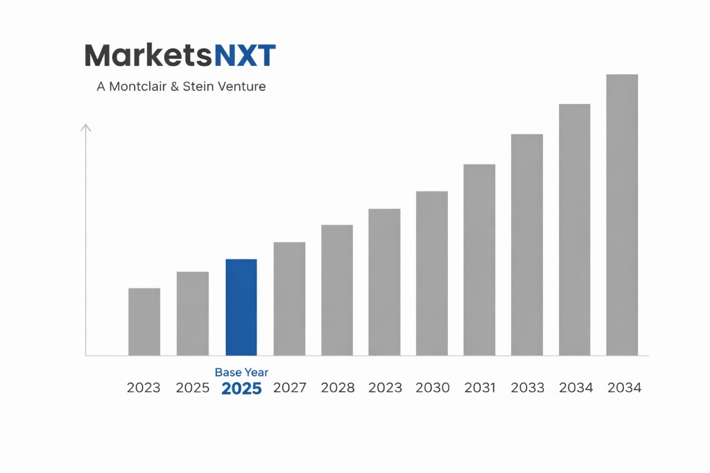
- ✓Market Size 2024: USD 1.8 billion
- ✓Market Size 2032: USD 3.2 billion
- ✓CAGR: 7.5%
- ✓Market Definition: Recovery and reprocessing of used silicon wafers from semiconductor manufacturing for reuse in production cycles
- ✓Leading Companies: Entegris, Rasa Industries, RS Technologies, Shin-Etsu Handotai, Siltronic
- ✓Base Year: 2025
- ✓Forecast Period: 2026-2032
China Silicon Wafer Reclaim: Market Overview
China's silicon wafer reclaim market represents a critical component of the country's semiconductor manufacturing ecosystem, valued at USD 1.8 billion in 2024. The market encompasses the collection, processing, and restoration of used silicon wafers from fabrication facilities, primarily serving the memory, logic, and power semiconductor sectors. Government policies prioritizing semiconductor self-sufficiency have elevated wafer reclaim from a cost-reduction measure to a strategic imperative for supply chain security.
The market structure reflects China's broader semiconductor industry dynamics, with state-owned enterprises and private companies competing alongside foreign technology providers. Government-backed semiconductor manufacturing expansion has created unprecedented volumes of reclaimable wafer material, while environmental regulations mandate responsible handling of semiconductor waste. The Ministry of Industry and Information Technology's semiconductor development guidelines specifically identify wafer reclaim as a priority area for technological advancement and capacity building.
Policy-Driven Growth in the silicon wafer reclaim sector
The National Integrated Circuit Industry Development Guidelines 2014-2030 allocate RMB 139.5 billion specifically for semiconductor manufacturing infrastructure, with wafer reclaim facilities receiving priority funding status. The China Integrated Circuit Industry Investment Fund's Phase II committed RMB 28.6 billion to semiconductor materials and equipment sectors, directly subsidizing wafer reclaim technology development. Additionally, the Circular Economy Promotion Law of 2018 mandates 85% material recovery rates for semiconductor manufacturing waste by 2025, creating regulatory demand for reclaim services.
Provincial governments supplement national policies with targeted incentives, including Jiangsu Province's semiconductor materials subsidy programme providing up to RMB 50 million per facility for wafer reclaim operations. The Ministry of Ecology and Environment's National Sword Policy restricts semiconductor waste exports, forcing domestic processing and driving reclaim market expansion. Tax incentives under the Enterprise Income Tax Law provide 15% preferential rates for high-tech wafer reclaim companies, reducing operational costs and accelerating market entry for qualified firms.
Regulatory Barriers and Compliance Costs
The State Administration for Market Regulation requires comprehensive licensing for wafer reclaim operations, with approval processes averaging 18-24 months and costing RMB 2.8-4.2 million per facility. Environmental impact assessments mandated by the Ministry of Ecology and Environment add 6-12 months to project timelines, requiring specialized wastewater treatment systems costing RMB 15-25 million per facility. The National Development and Reform Commission's industrial policy catalog restricts foreign ownership in wafer reclaim to 49%, limiting international investment and technology transfer.
Quality certification requirements from the China National Accreditation Service demand ISO 14001 environmental management and IATF 16949 automotive quality standards for automotive-grade reclaim operations, adding RMB 800,000-1.2 million in annual compliance costs. The Ministry of Commerce's export control regulations on semiconductor materials require export licenses for reclaimed wafers above 200mm diameter, creating administrative delays of 30-45 days for international sales. Local content requirements mandate 60% domestic equipment usage in new reclaim facilities by 2026, increasing capital expenditure by an estimated 25-30%.
Policy-Created Opportunities in China
The Made in China 2025 strategy creates substantial procurement opportunities through state-owned semiconductor manufacturers, with China National Electronics Corporation and Tsinghua Unigroup committing to source 70% of reclaim services domestically by 2027. The National Smart Manufacturing Development Plan designates wafer reclaim as a priority automation sector, providing RMB 500 million in Industry 4.0 upgrade subsidies for qualifying facilities. Regional development policies in Hefei, Wuxi, and Shenzhen offer land-use rights at 40-60% below market rates for wafer reclaim operations supporting local semiconductor clusters.
The Dual Carbon Policy framework creates additional opportunities through carbon credit mechanisms for waste reduction in semiconductor manufacturing, with reclaim operations eligible for certified emission reduction credits worth RMB 150-200 per tonne CO2 equivalent. The Ministry of Finance's green bond programme provides preferential financing rates of 2.5-3.5% for environmentally beneficial wafer reclaim projects, compared to standard commercial rates of 4.8-6.2%. Cross-border e-commerce regulations facilitate reclaim service exports to Belt and Road Initiative countries, with simplified customs procedures and reduced administrative barriers for registered service providers.
Market at a Glance
| Metric | Value |
|---|---|
| Market Size 2024 | USD 1.8 billion |
| Market Size 2032 | USD 3.2 billion |
| Growth Rate (CAGR) | 7.5% |
| Most Critical Decision Factor | Regulatory compliance and quality certification |
| Largest Region | Yangtze River Delta |
| Competitive Structure | Consolidated with emerging domestic players |
Leading Market Participants
- Entegris
- Rasa Industries
- RS Technologies
- Shin-Etsu Handotai
- Siltronic
- SUMCO Corporation
- Ferrotec Holdings
- Pure Wafer
- Noel Technologies
- KST World Corporation
Regulatory and Policy Environment
China's wafer reclaim industry operates under the Measures for the Administration of Waste Electrical and Electronic Equipment Processing Qualification, administered by the Ministry of Ecology and Environment, which establishes mandatory processing standards and facility certification requirements. The regulation requires annual audits costing RMB 200,000-400,000 and maintains strict contamination limits of less than 0.1 parts per billion for metallic impurities in reclaimed wafers. The National Development and Reform Commission's Catalogue for Guidance of Foreign Investment Industries restricts foreign participation while encouraging technology transfer through joint ventures with domestic partners.
Upcoming regulatory changes include the revised Solid Waste Pollution Prevention and Control Law implementation in 2025, mandating real-time monitoring systems for all wafer reclaim operations and establishing criminal liability for non-compliance. China's regulatory framework differs significantly from regional peers, with stricter environmental monitoring requirements than Taiwan and South Korea but more flexible foreign investment terms than Japan. The State Council's semiconductor industry development plan requires domestic wafer reclaim capacity to reach 2.5 million wafers per month by 2030, supported by preferential policies including accelerated depreciation schedules and research and development tax credits reaching 200% of qualifying expenses.
Long-Term Policy Outlook for silicon wafer reclaim in China
Policy developments through 2032 will likely emphasize technological self-reliance and environmental sustainability, with the 15th Five-Year Plan expected to mandate advanced reclaim technologies for 300mm wafers and establish national quality standards equivalent to virgin wafer specifications. The Ministry of Science and Technology's semiconductor materials roadmap targets breakthrough achievements in ion implantation removal and epitaxial layer restoration by 2028, supported by RMB 2.1 billion in directed research funding. Carbon neutrality commitments will drive stricter energy efficiency standards for reclaim operations, potentially requiring renewable energy sourcing for 80% of facility power consumption by 2030.
Geopolitical considerations will reshape policy frameworks, with export control regulations likely expanding to include reclaim technologies above 28nm process nodes and strategic material recovery capabilities. The National Security Law's technology review mechanisms may require government approval for foreign technology licensing in advanced reclaim processes, while domestic content requirements could reach 85% for all reclaim equipment by 2032. Regional integration policies under the Regional Comprehensive Economic Partnership will facilitate cross-border reclaim services with ASEAN countries, creating opportunities for Chinese companies to establish processing centers serving regional semiconductor hubs while maintaining compliance with evolving technology transfer restrictions.
Frequently Asked Questions
Market Segmentation
- 150mm
- 200mm
- 300mm
- 450mm
- Memory Devices
- Logic Devices
- Power Semiconductors
- MEMS
- RF Devices
- Optical Devices
- Chemical Mechanical Polishing
- Wet Chemical Etching
- Plasma Etching
- Thermal Treatment
- Integrated Device Manufacturers
- Foundries
- Memory Manufacturers
- Discrete Device Manufacturers
- Test and Measurement
Table of Contents
1.1 Research Methodology
1.2 Scope and Definitions
1.3 Data Sources Chapter 02 Executive Summary
2.1 Report Highlights
2.2 Market Size and Forecast 2024-2032 Chapter 03 China Silicon Wafer Reclaim Market - Market Analysis
3.1 Market Overview
3.2 Growth Drivers
3.3 Restraints
3.4 Opportunities Chapter 04 Wafer Size Insights
4.1 150mm
4.2 200mm
4.3 300mm
4.4 450mm Chapter 05 Application Insights
5.1 Memory Devices
5.2 Logic Devices
5.3 Power Semiconductors
5.4 MEMS
5.5 RF Devices
5.6 Optical Devices Chapter 06 Reclaim Process Insights
6.1 Chemical Mechanical Polishing
6.2 Wet Chemical Etching
6.3 Plasma Etching
6.4 Thermal Treatment Chapter 07 End User Insights
7.1 Integrated Device Manufacturers
7.2 Foundries
7.3 Memory Manufacturers
7.4 Discrete Device Manufacturers
7.5 Test and Measurement Chapter 08 Competitive Landscape
8.1 Market Players
8.2 Leading Market Participants
8.2.1 Entegris
8.2.2 Rasa Industries
8.2.3 RS Technologies
8.2.4 Shin-Etsu Handotai
8.2.5 Siltronic
8.2.6 SUMCO Corporation
8.2.7 Ferrotec Holdings
8.2.8 Pure Wafer
8.2.9 Noel Technologies
8.2.10 KST World Corporation
8.3 Regulatory Environment
8.4 Outlook
Research Framework and Methodological Approach
Information
Procurement
Information
Analysis
Market Formulation
& Validation
Overview of Our Research Process
MarketsNXT follows a structured, multi-stage research framework designed to ensure accuracy, reliability, and strategic relevance of every published study. Our methodology integrates globally accepted research standards with industry best practices in data collection, modeling, verification, and insight generation.
1. Data Acquisition Strategy
Robust data collection is the foundation of our analytical process. MarketsNXT employs a layered sourcing model.
- Company annual reports & SEC filings
- Industry association publications
- Technical journals & white papers
- Government databases (World Bank, OECD)
- Paid commercial databases
- KOL Interviews (CEOs, Marketing Heads)
- Surveys with industry participants
- Distributor & supplier discussions
- End-user feedback loops
- Questionnaires for gap analysis
Analytical Modeling and Insight Development
After collection, datasets are processed and interpreted using multiple analytical techniques to identify baseline market values, demand patterns, growth drivers, constraints, and opportunity clusters.
2. Market Estimation Techniques
MarketsNXT applies multiple estimation pathways to strengthen forecast accuracy.
Bottom-up Approach
Aggregating granular demand data from country level to derive global figures.
Top-down Approach
Breaking down the parent industry market to identify the target serviceable market.
Supply Chain Anchored Forecasting
MarketsNXT integrates value chain intelligence into its forecasting structure to ensure commercial realism and operational alignment.
Supply-Side Evaluation
Revenue and capacity estimates are developed through company financial reviews, product portfolio mapping, benchmarking of competitive positioning, and commercialization tracking.
3. Market Engineering & Validation
Market engineering involves the triangulation of data from multiple sources to minimize errors.
Extensive gathering of raw data.
Statistical regression & trend analysis.
Cross-verification with experts.
Publication of market study.
Client-Centric Research Delivery
MarketsNXT positions research delivery as a collaborative engagement rather than a static information transfer. Analysts work with clients to clarify objectives, interpret findings, and connect insights to strategic decisions.