
France Semiconductor IP Market Size, Share & Forecast 2026–2034
Report Highlights
- ✓France: Semiconductor IP Market
- ✓Market Size 2024: $1.2 billion
- ✓Market Size 2032: $2.8 billion
- ✓CAGR: 11.2%
- ✓Base Year: 2025
- ✓Forecast Period: 2026-2032
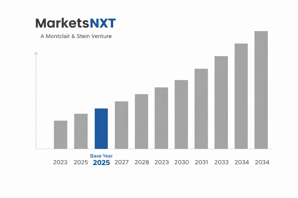
France Semiconductor IP Market: Market Overview
The French semiconductor intellectual property market represents a critical component of Europe's broader digital sovereignty strategy, valued at $1.2 billion in 2024. The market encompasses processor IP, interface IP, memory compilers, and verification IP, with government-backed initiatives like France Relance and the European Chips Act driving substantial investment in domestic semiconductor capabilities. French companies like Dolphin Design and Tiempo Secure have established strong positions in specialized IP segments, while international players maintain significant market presence through local partnerships and research collaborations.
Policy intervention has fundamentally reshaped market dynamics, with the French government's Plan Quantique allocating €1.8 billion toward quantum and semiconductor technologies through 2025. State-owned investment vehicle Bpifrance has co-invested in multiple semiconductor IP ventures, while the National Research Agency (ANR) provides targeted funding for IP development projects. This policy framework has created a hybrid market structure where government priorities increasingly influence private sector investment decisions and technology roadmaps.
Policy-Driven Growth in the French Semiconductor IP Market
The France 2030 investment plan designates €6 billion for digital and semiconductor technologies, with specific provisions for semiconductor IP development under the "Securing digital technology and telecommunications value chains" priority. The Loi de Programmation Militaire 2024-2030 mandates increased use of European semiconductor IP in defense applications, creating guaranteed demand worth an estimated €400 million annually. Additionally, the European Chips Act's implementation through French legislation requires public procurement entities to prioritize EU-sourced semiconductor IP when available, effectively creating protected market segments for domestic providers.
The Crédit Impôt Recherche (CIR) tax credit provides up to 30% reduction on R&D expenses for semiconductor IP development, directly reducing development costs for French companies. The government's Digital Transition Plan includes semiconductor IP in its strategic sectors list, enabling accelerated depreciation schedules and preferential loan terms through Bpifrance. These mechanisms translate into approximately 15-20% cost advantages for French IP developers compared to purely commercial financing options, driving increased domestic investment and market expansion.
Regulatory Barriers and Compliance Costs
The Commission Nationale de l'Informatique et des Libertés (CNIL) enforces strict data protection requirements for semiconductor IP containing embedded security features, requiring compliance audits that typically cost €50,000-200,000 per IP core. The Agence Nationale de la Sécurité des Systèmes d'Information (ANSSI) maintains export control classifications for dual-use semiconductor IP, with approval processes extending 3-6 months for sensitive technologies. Additionally, the Direction Générale de l'Armement (DGA) requires security clearance for IP developers working on defense-related projects, creating workforce constraints and additional compliance overhead.
Environmental regulations under the French Energy Transition Law require lifecycle carbon assessments for semiconductor IP used in consumer electronics, adding approximately €30,000-50,000 in certification costs per major IP release. The French competition authority (Autorité de la Concurrence) maintains heightened scrutiny of semiconductor IP licensing agreements, particularly those involving essential patents, leading to extended legal review periods of 6-12 months for complex cross-licensing arrangements. These regulatory requirements create particular challenges for smaller IP developers lacking dedicated compliance resources.
Policy-Created Opportunities in France
The forthcoming Sovereign Semiconductor Initiative, announced for 2025 implementation, will establish government-guaranteed purchase agreements worth €2.5 billion for French-developed semiconductor IP over five years. The initiative prioritizes automotive, aerospace, and telecommunications applications, creating predictable demand streams that enable long-term investment planning. Concurrently, the Ministry of Higher Education's quantum computing roadmap includes €600 million in targeted funding for quantum-compatible semiconductor IP development, representing a nascent but high-value market segment with limited global competition.
Regional development policies offer additional opportunities, with the Auvergne-Rhône-Alpes region providing up to €10 million in co-funding for semiconductor IP clusters, while Nouvelle-Aquitaine's aerospace focus creates dedicated funding streams for avionics-specific IP development. The government's proposed modification to public procurement rules, expected in 2026, will allow contracting authorities to weight local content up to 25% in bid evaluations, effectively creating preferential access for French IP providers in public sector projects worth approximately €800 million annually.
Market at a Glance
| Metric | Value |
|---|---|
| Market Size 2024 | $1.2 billion |
| Market Size 2032 | $2.8 billion |
| Growth Rate (CAGR) | 11.2% |
| Most Critical Decision Factor | Government procurement requirements |
| Largest Region | Île-de-France |
| Competitive Structure | Fragmented with policy-driven consolidation |
Leading Market Participants
- Dolphin Design
- Tiempo Secure
- Arteris
- ARM Limited
- Synopsys
- Cadence Design Systems
- Lattice Semiconductor
- eMemory Technology
- Rambus
- Mentor Graphics
Regulatory and Policy Environment
The Loi de Programmation sur la Recherche 2021-2030 serves as the primary legislative framework governing semiconductor IP development in France, administered by the Ministry of Higher Education, Research and Innovation. Key compliance requirements include mandatory reporting of foreign investment in semiconductor IP companies exceeding €1 million, technology transfer agreements subject to prior approval by the Direction Générale des Entreprises (DGE), and adherence to EU state aid rules for government-supported IP development projects. The forthcoming European Chips Act implementation, expected by mid-2025, will introduce additional notification requirements for strategic semiconductor IP transactions and establish preferential procurement mechanisms favoring EU suppliers.
France's regulatory framework differs significantly from regional peers through its emphasis on defense applications and quantum readiness requirements. Unlike Germany's primarily economic approach or the Netherlands' export control focus, French regulations integrate national security considerations into commercial IP development through the Commission d'Examen des Investissements Étrangers (CFIUS equivalent). Upcoming regulatory changes include strengthened foreign direct investment screening for semiconductor IP acquisitions, new cybersecurity certification requirements for IP cores used in critical infrastructure, and revised tax incentives specifically targeting quantum-compatible semiconductor technologies, all scheduled for implementation between 2025-2027.
Long-Term Policy Outlook for French Semiconductor IP
The French government's 2032 strategic autonomy objectives will likely drive further market intervention through expanded public procurement preferences and increased R&D funding specifically targeting semiconductor IP. The planned European Sovereignty Fund, with French contributions of €2 billion, is expected to prioritize semiconductor IP projects that reduce dependencies on non-EU suppliers. Additionally, the government's quantum computing ambitions require substantial semiconductor IP development capabilities, with policy makers indicating willingness to provide direct subsidies and preferential market access to achieve technological leadership by 2030.
Climate policy integration represents another major policy trend, with the forthcoming Green Digital Strategy requiring semiconductor IP to meet strict energy efficiency standards by 2028. This will likely create market advantages for French companies already developing low-power IP solutions while potentially limiting market access for high-consumption alternatives. The government's commitment to achieving 40% domestic content in critical semiconductor applications by 2032 suggests continued policy support for French IP providers, including potential mandatory local content requirements in defense and infrastructure projects.
Frequently Asked Questions
Market Segmentation
- Processor IP
- Interface IP
- Memory Compiler
- Platform IP
- Verification IP
- Automotive
- Consumer Electronics
- Industrial
- Telecommunications
- Aerospace & Defense
- Computing & Storage
- Licensing
- Royalty
- Hybrid
- Semiconductor Companies
- System Companies
- Fabless Companies
- Research Institutions
Table of Contents
Chapter 01 Methodology and Scope
Chapter 02 Executive Summary
Chapter 03 France Semiconductor IP Market - Market Analysis
3.1 Market Overview / 3.2 Growth Drivers / 3.3 Restraints / 3.4 Opportunities
Chapter 04 IP Type Insights
Chapter 05 Application Insights
Chapter 06 Revenue Model Insights
Chapter 07 End User Insights
Chapter 08 Competitive Landscape
8.1 Market Players / 8.2 Leading Market Participants / 8.3 Regulatory Environment / 8.4 Outlook
Research Framework and Methodological Approach
Information
Procurement
Information
Analysis
Market Formulation
& Validation
Overview of Our Research Process
MarketsNXT follows a structured, multi-stage research framework designed to ensure accuracy, reliability, and strategic relevance of every published study. Our methodology integrates globally accepted research standards with industry best practices in data collection, modeling, verification, and insight generation.
1. Data Acquisition Strategy
Robust data collection is the foundation of our analytical process. MarketsNXT employs a layered sourcing model.
- Company annual reports & SEC filings
- Industry association publications
- Technical journals & white papers
- Government databases (World Bank, OECD)
- Paid commercial databases
- KOL Interviews (CEOs, Marketing Heads)
- Surveys with industry participants
- Distributor & supplier discussions
- End-user feedback loops
- Questionnaires for gap analysis
Analytical Modeling and Insight Development
After collection, datasets are processed and interpreted using multiple analytical techniques to identify baseline market values, demand patterns, growth drivers, constraints, and opportunity clusters.
2. Market Estimation Techniques
MarketsNXT applies multiple estimation pathways to strengthen forecast accuracy.
Bottom-up Approach
Aggregating granular demand data from country level to derive global figures.
Top-down Approach
Breaking down the parent industry market to identify the target serviceable market.
Supply Chain Anchored Forecasting
MarketsNXT integrates value chain intelligence into its forecasting structure to ensure commercial realism and operational alignment.
Supply-Side Evaluation
Revenue and capacity estimates are developed through company financial reviews, product portfolio mapping, benchmarking of competitive positioning, and commercialization tracking.
3. Market Engineering & Validation
Market engineering involves the triangulation of data from multiple sources to minimize errors.
Extensive gathering of raw data.
Statistical regression & trend analysis.
Cross-verification with experts.
Publication of market study.
Client-Centric Research Delivery
MarketsNXT positions research delivery as a collaborative engagement rather than a static information transfer. Analysts work with clients to clarify objectives, interpret findings, and connect insights to strategic decisions.