India Extreme Ultraviolet (EUV) Lithography Market Size, Share & Forecast 2026–2034
Report Highlights
- ✓Country: India
- ✓Market: Extreme Ultraviolet (EUV) Lithography
- ✓Market Size 2024: USD 148 million
- ✓Market Size 2032: USD 1.02 billion
- ✓CAGR: 27.1%
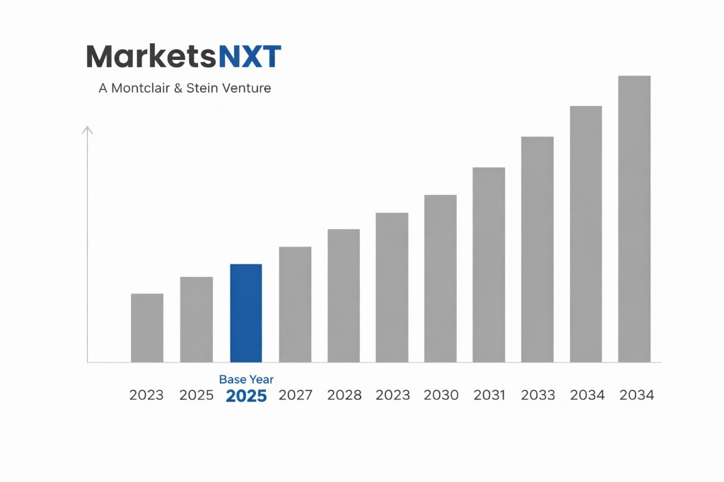
- ✓Base Year: 2025
- ✓Forecast Period: 2026–2032
Analyst Recommendation — Secure Tool Allocation Now: Investors entering the India EUV market should negotiate ASML tool allocation agreements before 2026, when global High-NA EUV demand will crowd out mid-tier buyers. Tying allocations to the ISM subsidy framework at Dholera locks in both supply access and government co-investment.
India Extreme Ultraviolet Lithography: Market Overview
India's EUV lithography market occupies a uniquely early-stage but high-velocity position within the global semiconductor equipment landscape. The domestic market, valued at USD 148 million in 2024, is almost entirely driven by government-backed semiconductor fabrication initiatives rather than existing commercial fab demand, distinguishing it sharply from mature markets in Taiwan, South Korea, and the United States where EUV adoption is driven by high-volume production at sub-7nm nodes. India's structural position as a dominant chip design hub with negligible domestic fabrication capacity creates an asymmetric market, where demand-side sophistication significantly outpaces supply-side infrastructure.
The India Semiconductor Mission, launched under the Semicon India Programme with an INR 76,000 crore (approximately USD 10 billion) incentive package, is the single most significant structural force shaping EUV market development in the country. Tata Electronics' planned fab at Dholera in Gujarat and CG Power's ATMP facility at Sanand represent the first wave of investments that will ultimately require EUV-capable process nodes to remain competitive beyond 28nm geometries. India's EUV market structure therefore differs from global norms in that policy commitment, not commercial backlog, is the primary demand signal for equipment investment decisions through at least 2028.
Growth Drivers in the India EUV Lithography Market
The India Semiconductor Mission's Production Linked Incentive structure, which offers up to 50% fiscal support on capital expenditure for eligible semiconductor fabs, creates a direct subsidy corridor for EUV tool procurement that reduces the effective cost barrier for first-mover entrants. The Ministry of Electronics and Information Technology's Semicon India Programme 2.0 discussions, ongoing through 2024, indicate a likely expansion of eligible node geometries to include sub-10nm processes, which directly mandates EUV adoption. These policy mechanisms are country-specific and have no equivalent in competing Southeast Asian markets, giving India a distinctive demand-pull dynamic for advanced lithography investment.
India's demographic and educational infrastructure provides a second structural driver. With over 85 semiconductor-focused academic institutions and IIT campuses running dedicated VLSI and nanoelectronics programmes, India produces approximately 40,000 chip design graduates annually. This talent pipeline reduces operating cost risk for fabs deploying EUV at scale and makes India attractive to multinational EUV process developers seeking to establish Asia-Pacific research partnerships. Additionally, the 2023 India-US Initiative on Critical and Emerging Technology (iCET) has explicitly identified semiconductor supply chain cooperation as a priority, positioning India as a strategic partner for US-aligned EUV technology access outside ASML's standard commercial queue.
Market Restraints and Entry Barriers
The single largest structural barrier to EUV market development in India is ASML's export control environment. ASML EUV systems require Dutch government export licenses, and the Netherlands has progressively tightened dual-use technology export regulations under US diplomatic pressure since 2023. India, while not explicitly restricted, is not a member of the Wassenaar Arrangement, which means each ASML EUV shipment to an Indian facility requires individual license review rather than blanket approval. This creates procurement timelines of 18 to 36 months per tool, compared to 6 to 12 months for approved-destination fabs in Japan or the Netherlands, materially elevating project execution risk for domestic fab developers at Dholera and Sanand.
Infrastructure deficits compound the regulatory barrier. EUV lithography systems require sub-nanometer vibration isolation, ultra-pure water systems delivering 18 megohm-cm resistivity, and cleanroom environments at ISO Class 1 or better. India currently has no operational fab facility that meets these specifications outside ISRO's limited-purpose cleanroom infrastructure at Thiruvananthapuram. Power supply reliability in Gujarat's Dholera Special Investment Region, the primary planned fab location, remains a risk factor, with grid stability metrics well below the 99.9999% uptime standard that EUV operations require. These infrastructure gaps translate into an estimated INR 8,000 to 12,000 crore in pre-fab site preparation costs per greenfield EUV-capable facility.
Market Opportunities in India EUV Lithography
The most immediate addressable opportunity lies in EUV-adjacent infrastructure supply: photomask blanks, pellicle components, high-purity chemical mechanical planarization slurries, and EUV-compatible photoresists. These upstream consumables represent a USD 38 to 52 million near-term opportunity by 2027, and Indian chemical manufacturers such as Jubilant Ingrevia and Himadri Speciality Chemical are already positioned with base chemistry capabilities that can be redirected toward semiconductor-grade material production with targeted capital investment. Entry into this segment requires substantially lower regulatory clearance thresholds than direct EUV tool import and offers faster time-to-revenue against the backdrop of ISM-funded fab construction timelines.
A second distinct opportunity exists in EUV metrology and inspection services. As Tata Electronics and future fab entrants move toward sub-28nm process qualification, demand for EUV scanner calibration, reticle inspection, and optical proximity correction modelling will require either imported services or a domestic service ecosystem. KLA Corporation and Onto Innovation have both signalled India market development interest in semiconductor process control, and a joint venture or local service entity structured around ISM's Design Linked Incentive scheme qualifies for government co-funding. This creates a USD 15 to 25 million addressable metrology services market by 2029 that carries materially lower capital intensity than fab equipment ownership.
Market at a Glance
| Metric | Detail |
|---|---|
| Market Size 2024 | USD 148 million |
| Market Size 2032 | USD 1.02 billion |
| Growth Rate (CAGR) | 27.1% |
| Most Critical Decision Factor | ASML export license approval timeline for India |
| Largest Region | Gujarat (Dholera Special Investment Region) |
| Competitive Structure | Nascent, policy-driven, single dominant equipment supplier |
Leading Market Participants
- ASML Holding N.V.
- Tata Electronics Private Limited
- Applied Materials India
- Lam Research India
- KLA India
- Tokyo Electron Limited (TEL)
- Onto Innovation
- Entegris India
- Shin-Etsu Chemical (India operations)
- Micron Technology India
Regulatory and Policy Environment
The primary legislative framework governing EUV equipment import and operation in India is the Foreign Trade (Development and Regulation) Act 1992, under which the Directorate General of Foreign Trade administers Special Chemicals, Organisms, Materials, Equipment and Technologies (SCOMET) export-import controls. EUV lithography systems are classified under SCOMET Category 3B001, requiring end-use certificates and post-shipment verification. The Ministry of Electronics and Information Technology administers the Semicon India Programme through a modified project approval process under the Modified Special Incentive Package Scheme (M-SIPS) successor framework, with capital subsidy disbursements tied to verified capital expenditure milestones and nodal agency sign-off from the India Semiconductor Mission Secretariat.
The iCET framework signed in June 2023 between Prime Minister Modi and President Biden commits both governments to facilitating semiconductor technology transfer and export review fast-tracking, which has prompted the US Department of Commerce's Bureau of Industry and Security to engage on licensing pathway simplification for India-bound EUV-adjacent equipment. The Semiconductor Ecosystem Development Fund, announced under Union Budget 2024-25 with INR 6,903 crore in allocation, specifically earmarks capital for advanced process node equipment procurement by ISM-approved entities. Compliance timelines for ISM-funded fabs mandate first-silicon milestones within 5 years of project sanction, creating a hard 2029 deadline for EUV tool installation and qualification at Dholera.
Long-Term Outlook for India EUV Lithography
By 2032, India's EUV lithography market is projected to reach USD 1.02 billion, driven primarily by second-generation fab expansion at Dholera and anticipated greenfield announcements from Foxconn's India semiconductor partnerships and potential ISMC revival under revised foreign direct investment terms. The market will bifurcate into a government-subsidised advanced node fabrication segment operating at sub-14nm geometries and a broader EUV-services ecosystem encompassing photomask handling, metrology, photoresist chemistry, and process engineering consultancy. This bifurcation mirrors South Korea's development trajectory in the late 2000s, where Samsung's government-backed advanced node push catalysed a domestic supply chain within eight years.
India's long-term competitive position in EUV lithography will be determined by two variables that remain unresolved: ASML tool allocation priority relative to competing Asian fab clusters, and the speed of India's Wassenaar Arrangement observer status or equivalent bilateral technology access agreement. If iCET negotiations produce an effective technology access corridor by 2027, India's EUV market will accelerate toward a self-sustaining commercial phase before 2032. If access remains constrained, the market will remain policy-subsidised and structurally dependent on imported process know-how, limiting the ecosystem depth that would otherwise emerge from a mature domestic fab base operating at competitive global node densities.
Frequently Asked Questions
Market Segmentation
- EUV Light Sources
- Optical Systems and Mirrors
- Photomasks and Reticles
- Photoresists
- Metrology and Inspection Equipment
- Wafer Handling Systems
- Logic Semiconductors
- DRAM Memory
- NAND Flash Memory
- Power Devices
- Photonics and MEMS
- Sub-7nm
- 7nm to 14nm
- 14nm to 28nm
- Above 28nm (EUV-assisted)
- Government-Backed Fabs
- Private Integrated Device Manufacturers
- Research and Academic Institutions
- Fabless Design Houses (indirect demand)
Table of Contents
Research Framework and Methodological Approach
Information
Procurement
Information
Analysis
Market Formulation
& Validation
Overview of Our Research Process
MarketsNXT follows a structured, multi-stage research framework designed to ensure accuracy, reliability, and strategic relevance of every published study. Our methodology integrates globally accepted research standards with industry best practices in data collection, modeling, verification, and insight generation.
1. Data Acquisition Strategy
Robust data collection is the foundation of our analytical process. MarketsNXT employs a layered sourcing model.
- Company annual reports & SEC filings
- Industry association publications
- Technical journals & white papers
- Government databases (World Bank, OECD)
- Paid commercial databases
- KOL Interviews (CEOs, Marketing Heads)
- Surveys with industry participants
- Distributor & supplier discussions
- End-user feedback loops
- Questionnaires for gap analysis
Analytical Modeling and Insight Development
After collection, datasets are processed and interpreted using multiple analytical techniques to identify baseline market values, demand patterns, growth drivers, constraints, and opportunity clusters.
2. Market Estimation Techniques
MarketsNXT applies multiple estimation pathways to strengthen forecast accuracy.
Bottom-up Approach
Aggregating granular demand data from country level to derive global figures.
Top-down Approach
Breaking down the parent industry market to identify the target serviceable market.
Supply Chain Anchored Forecasting
MarketsNXT integrates value chain intelligence into its forecasting structure to ensure commercial realism and operational alignment.
Supply-Side Evaluation
Revenue and capacity estimates are developed through company financial reviews, product portfolio mapping, benchmarking of competitive positioning, and commercialization tracking.
3. Market Engineering & Validation
Market engineering involves the triangulation of data from multiple sources to minimize errors.
Extensive gathering of raw data.
Statistical regression & trend analysis.
Cross-verification with experts.
Publication of market study.
Client-Centric Research Delivery
MarketsNXT positions research delivery as a collaborative engagement rather than a static information transfer. Analysts work with clients to clarify objectives, interpret findings, and connect insights to strategic decisions.