Indonesia Extreme Ultraviolet (EUV) Lithography Market Size, Share & Forecast 2026–2034
Report Highlights
- ✓Market Size 2024: USD 45.2 million
- ✓Market Size 2032: USD 312.8 million
- ✓CAGR: 27.4%
- ✓Market Definition: Advanced semiconductor manufacturing equipment and services utilizing extreme ultraviolet light wavelengths (13.5 nm) for producing chips with feature sizes below 7nm, encompassing lithography systems, photomasks, photoresists, and related process technologies essential for next-generation semiconductor fabrication in Indonesia's emerging high-tech manufacturing sector.
- ✓Leading Companies: ASML Holding, Taiwan Semiconductor Manufacturing, Samsung Electronics, Intel Corporation, Applied Materials
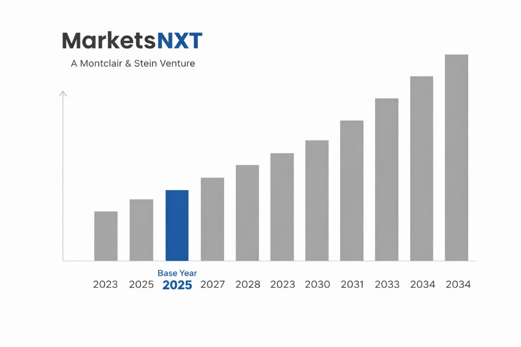
- ✓Base Year: 2025
- ✓Forecast Period: 2026-2032
Analyst Recommendation — Secure Early Partnerships: Semiconductor equipment buyers should establish supplier agreements with Indonesian precision manufacturers by Q2 2026, before anticipated government incentives for local content requirements in EUV supply chains take effect and limit foreign sourcing options.
Indonesia's Role in the Global EUV Lithography Supply Chain
Indonesia occupies a nascent but strategically important position in the global EUV lithography supply chain, primarily as an emerging assembly and packaging hub for advanced semiconductors manufactured using EUV technology. The country currently imports 100% of its EUV-related equipment, with ASML systems entering through Singapore and South Korea for deployment at multinational semiconductor facilities. Taiwan Semiconductor Manufacturing Company's USD 2.8 billion investment in Batam represents the first major EUV-adjacent facility, focusing on advanced packaging for chips manufactured using EUV processes at TSMC's Taiwan and Arizona fabs. This positions Indonesia as a critical link between EUV chip production and final product assembly for consumer electronics destined for Southeast Asian markets.
The country's supply chain role extends beyond assembly to precision component manufacturing for EUV systems. Indonesian manufacturers, particularly in the Bekasi and Karawang industrial corridors, are developing capabilities in ultra-clean manufacturing environments required for EUV photomask handling systems and metrology equipment. Local firms like PT Dirgantara Indonesia and PT Pindad are leveraging aerospace-grade precision manufacturing expertise to produce components for EUV system peripherals. Singapore serves as the primary transshipment hub, handling 78% of EUV equipment imports destined for Indonesia, while direct shipments from the Netherlands account for 22% of high-value ASML system components entering Jakarta's Soekarno-Hatta cargo facilities.
Growth Drivers for Indonesian EUV Lithography Trade and Production
Government industrial policy represents the primary driver for Indonesia's EUV market expansion, with the Making Indonesia 4.0 initiative allocating USD 1.2 billion specifically for semiconductor ecosystem development through 2030. The Ministry of Industry's semiconductor roadmap mandates local content requirements increasing from 5% in 2026 to 25% by 2030 for advanced semiconductor manufacturing equipment, creating guaranteed demand for domestically produced EUV peripheral components. Tax incentives including 100% depreciation allowances for EUV equipment purchases and 15-year tax holidays for semiconductor facilities processing sub-10nm chips are attracting foreign direct investment from Asian semiconductor giants seeking cost-effective advanced packaging locations.
Regional supply chain diversification efforts by multinational corporations drive substantial equipment demand as companies reduce China dependency following US export controls. Samsung Electronics' planned USD 1.8 billion memory packaging facility in Cikarang specifically targets EUV-manufactured memory chips, requiring significant investments in EUV-compatible metrology and inspection equipment. The Indonesia-Japan Comprehensive Economic Partnership Agreement provides preferential tariff treatment for EUV equipment imports, reducing total landed costs by 12-15% compared to other Southeast Asian destinations. Additionally, Indonesia's strategic location enables efficient distribution of EUV-packaged semiconductors to growing markets in India, Australia, and emerging economies throughout the Indian Ocean region.
Supply Chain Risks and Trade Barriers
Critical infrastructure limitations pose significant risks to Indonesia's EUV supply chain ambitions, particularly regarding electrical grid stability and ultra-pure water supply systems essential for EUV operations. Power outages exceeding 30 minutes can damage EUV photoresist materials worth USD 500,000 per incident, while Indonesia's current grid reliability of 99.1% falls short of the 99.99% uptime required for continuous EUV processing. The country's dependence on Singapore's Changi Airport for air cargo handling creates bottlenecks during peak shipping periods, with EUV equipment deliveries experiencing 3-7 day delays during monsoon seasons when alternative routing through Kuala Lumpur becomes necessary. Limited cold storage facilities at Indonesian ports risk degradation of temperature-sensitive EUV photoresists and cleaning chemicals during customs clearance procedures.
Regulatory uncertainty surrounding technology transfer restrictions and export control compliance creates operational risks for multinational EUV equipment users. Indonesia's unclear interpretation of US Bureau of Industry and Security regulations regarding EUV technology sharing with Chinese partners has delayed several planned joint ventures, particularly affecting equipment maintenance contracts with ASML and Applied Materials. Currency volatility represents another significant risk, with the Indonesian rupiah's 8.5% depreciation against the US dollar in 2024 increasing EUV equipment costs and maintenance expenses. Additionally, limited availability of EUV-qualified technicians, with only 180 certified professionals nationwide compared to 2,400 in Singapore, creates dependency on expensive expatriate expertise and threatens operational continuity during visa processing delays or travel restrictions.
Trade and Investment Opportunities in Indonesia
Import substitution opportunities in EUV peripheral equipment manufacturing present substantial commercial potential, particularly in photomask handling systems, wafer transport mechanisms, and environmental monitoring equipment where local content requirements will mandate 25% domestic sourcing by 2030. Indonesian precision manufacturers can capture USD 85 million annually in EUV support equipment revenue by developing ultra-clean manufacturing capabilities and obtaining ISO 14644 Class 1 cleanroom certifications. Joint ventures between Indonesian firms and established EUV suppliers offer pathways to technology transfer while meeting government local partnership requirements. PT Krakatau Steel's planned specialty alloy division specifically targets EUV system component materials, representing a USD 200 million investment opportunity in high-purity metals essential for chamber construction and optical system mounting.
Export opportunities center on serving as a regional hub for EUV-packaged semiconductor distribution throughout Southeast Asia and the Indian Ocean region. Indonesia's Free Trade Zone status in Batam provides duty-free assembly and re-export capabilities for EUV-manufactured chips, while the country's ASEAN Trade in Goods Agreement enables preferential access to markets representing 650 million consumers. Logistics investment opportunities include specialized EUV equipment handling facilities at Tanjung Priok Port and dedicated cleanroom storage at Soekarno-Hatta Airport, with projected returns of 18-22% annually based on growing regional semiconductor trade volumes. The development of EUV-qualified workforce training centers presents additional opportunities, with government subsidies covering 70% of facility costs for programs meeting Ministry of Education certification standards.
Market at a Glance
| Parameter | Value |
|---|---|
| Market Size 2024 | USD 45.2 million |
| Market Size 2032 | USD 312.8 million |
| Growth Rate (CAGR) | 27.4% |
| Most Critical Decision Factor | Government local content mandates |
| Largest Region | Java Island Industrial Corridor |
| Competitive Structure | Foreign equipment dominance with emerging local assembly |
Leading Market Participants
- ASML Holding
- Taiwan Semiconductor Manufacturing
- Samsung Electronics
- Intel Corporation
- Applied Materials
- Tokyo Electron
- KLA Corporation
- Lam Research
- JSR Corporation
- Shin-Etsu Chemical
Regulatory and Trade Policy Environment
Indonesia's EUV lithography regulatory framework operates under the Making Indonesia 4.0 industrial transformation policy, which establishes semiconductor manufacturing as a national strategic priority with specific provisions for advanced lithography equipment. The Ministry of Industry's Regulation No. 23/2021 mandates local content requirements for semiconductor manufacturing equipment, escalating from 5% in 2026 to 25% by 2030, directly impacting EUV system procurement and installation. Investment incentives under Government Regulation No. 35/2021 provide 100% accelerated depreciation for EUV equipment purchases exceeding USD 50 million and 15-year corporate tax holidays for facilities achieving sub-10nm processing capabilities. The Indonesia-Singapore Comprehensive Economic Partnership Agreement facilitates equipment imports with reduced documentation requirements, while the Regional Comprehensive Economic Partnership provides preferential tariffs for EUV components from Japan and South Korea.
Export control compliance represents a critical regulatory challenge, with Indonesia implementing dual-use technology regulations aligned with Wassenaar Arrangement guidelines but lacking specific EUV technology classification frameworks. The National Agency for Export Control coordinates with international partners to ensure EUV equipment transfers comply with US Bureau of Industry and Security restrictions, particularly regarding Chinese entity list considerations. Foreign investment regulations under Law No. 11/2020 require technology transfer agreements for EUV-related investments exceeding USD 100 million, mandating knowledge sharing with local partners and workforce development commitments. Environmental regulations under Ministry of Environment Decree No. 5/2021 establish specific air quality and chemical handling standards for EUV facilities, requiring continuous monitoring systems and specialized waste treatment capabilities for photoresist and cleaning chemical disposal.
Indonesian EUV Lithography Supply Chain Outlook to 2032
Indonesia's EUV supply chain position will evolve from pure import dependency to a regional assembly and component manufacturing hub by 2032, with domestic production capabilities expected to capture 15-20% of the peripheral equipment market. The completion of TSMC's Batam facility in 2027 will establish Indonesia as Southeast Asia's primary advanced packaging center for EUV-manufactured chips, processing an estimated 40,000 wafer equivalents monthly by 2030. Local manufacturers will achieve ISO 14644 Class 1 cleanroom capabilities by 2028, enabling production of photomask handling systems, wafer transport equipment, and environmental monitoring devices for EUV applications. Government-backed technology transfer partnerships with Dutch and Japanese suppliers will result in three major joint venture facilities operational by 2029, producing EUV system components worth USD 180 million annually.
Trade flows will shift significantly as Indonesia develops export capabilities in EUV support equipment while maintaining import dependency for core lithography systems from ASML. The country's strategic position will enable efficient distribution of EUV-packaged semiconductors throughout the Indian Ocean region, with dedicated logistics hubs at Tanjung Priok and Batam handling 25% of regional semiconductor trade by 2032. Technology advancement will focus on developing indigenous capabilities in EUV metrology and inspection equipment, leveraging partnerships with local universities and international research institutions. The establishment of an EUV technology center in Bandung, supported by USD 150 million in government funding, will accelerate domestic innovation and position Indonesia as a regional expertise hub for next-generation lithography technologies beyond current EUV capabilities.
Frequently Asked Questions
Market Segmentation
- EUV Scanners
- Photomasks
- Photoresists
- Metrology Equipment
- Inspection Systems
- Support Equipment
- Logic Semiconductors
- Memory Devices
- Advanced Packaging
- Research and Development
- Semiconductor Foundries
- Integrated Device Manufacturers
- Assembly and Test Services
- Research Institutions
- Java Island
- Batam Industrial Zone
- Sumatra
- Other Regions
Table of Contents
Research Framework and Methodological Approach
Information
Procurement
Information
Analysis
Market Formulation
& Validation
Overview of Our Research Process
MarketsNXT follows a structured, multi-stage research framework designed to ensure accuracy, reliability, and strategic relevance of every published study. Our methodology integrates globally accepted research standards with industry best practices in data collection, modeling, verification, and insight generation.
1. Data Acquisition Strategy
Robust data collection is the foundation of our analytical process. MarketsNXT employs a layered sourcing model.
- Company annual reports & SEC filings
- Industry association publications
- Technical journals & white papers
- Government databases (World Bank, OECD)
- Paid commercial databases
- KOL Interviews (CEOs, Marketing Heads)
- Surveys with industry participants
- Distributor & supplier discussions
- End-user feedback loops
- Questionnaires for gap analysis
Analytical Modeling and Insight Development
After collection, datasets are processed and interpreted using multiple analytical techniques to identify baseline market values, demand patterns, growth drivers, constraints, and opportunity clusters.
2. Market Estimation Techniques
MarketsNXT applies multiple estimation pathways to strengthen forecast accuracy.
Bottom-up Approach
Aggregating granular demand data from country level to derive global figures.
Top-down Approach
Breaking down the parent industry market to identify the target serviceable market.
Supply Chain Anchored Forecasting
MarketsNXT integrates value chain intelligence into its forecasting structure to ensure commercial realism and operational alignment.
Supply-Side Evaluation
Revenue and capacity estimates are developed through company financial reviews, product portfolio mapping, benchmarking of competitive positioning, and commercialization tracking.
3. Market Engineering & Validation
Market engineering involves the triangulation of data from multiple sources to minimize errors.
Extensive gathering of raw data.
Statistical regression & trend analysis.
Cross-verification with experts.
Publication of market study.
Client-Centric Research Delivery
MarketsNXT positions research delivery as a collaborative engagement rather than a static information transfer. Analysts work with clients to clarify objectives, interpret findings, and connect insights to strategic decisions.