Japan Silicon Wafer Reclaim Market Size, Share & Forecast 2026–2034
Report Highlights
- ✓Country: Japan
- ✓Market: Silicon Wafer Reclaim Market
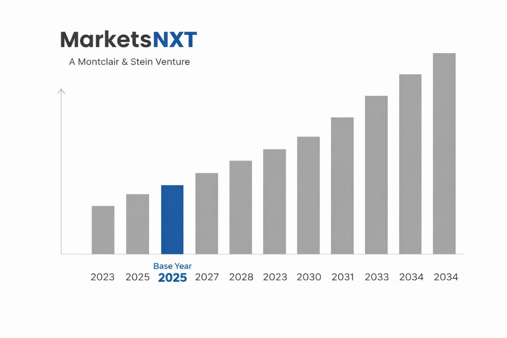
- ✓Market Size 2024: $450.2 million
- ✓Market Size 2032: $721.8 million
- ✓CAGR: 6.1%
- ✓Base Year: 2025
- ✓Forecast Period: 2026-2032
Japan Silicon Wafer Reclaim: Market Overview
Japan's silicon wafer reclaim market represents one of the world's most sophisticated and technologically advanced reclaim ecosystems, driven by the country's position as a global semiconductor manufacturing hub. The market is characterized by exceptionally high technical standards, with Japanese facilities achieving reclaim yields exceeding 95% for prime-grade wafers, significantly above global averages. Major semiconductor manufacturers including Sony, Renesas, and Rohm maintain dedicated reclaim partnerships with specialized service providers, creating a tightly integrated supply chain that prioritizes quality over cost reduction.
The Japanese market differs fundamentally from other regions through its emphasis on ultra-high precision reclaim processes and stringent contamination control standards mandated by the Japan Electronics and Information Technology Industries Association (JEITA). Japanese reclaim facilities operate under ISO 14001 environmental standards while achieving particle counts below 0.1 particles per cubic centimeter for 0.1-micron particles, enabling reclaimed wafers to meet the demanding specifications of advanced logic and memory production. This technical excellence has established Japan as a preferred destination for high-value reclaim services, particularly for 300mm wafers used in cutting-edge semiconductor applications.
Growth Drivers in the Japan Silicon Wafer Reclaim Market
The Japanese government's Strategic Innovation Program (SIP) for next-generation semiconductors, launched in 2022 with ¥77 billion in funding through 2030, directly supports advanced reclaim technologies as part of national supply chain resilience initiatives. This program incentivizes domestic semiconductor manufacturers to increase reclaim adoption through tax credits equivalent to 15% of reclaim service costs, while funding research partnerships between universities and reclaim service providers. Additionally, Japan's aging semiconductor fabrication facilities, with over 60% of domestic fabs exceeding 15 years of operation, generate substantial volumes of test wafers and production rejects suitable for reclaim processing.
Environmental regulations under Japan's Act on Promotion of Resource Circulation for Plastics, extended to semiconductor materials in 2023, mandate minimum 40% material recovery rates for silicon-containing manufacturing waste by 2027. The Japan Semiconductor Industry Association (JSIA) has established voluntary targets requiring member companies to achieve 65% wafer reclaim rates by 2030, driving systematic adoption across the industry. Demographic factors also contribute significantly, as Japan's shrinking workforce in semiconductor manufacturing creates labor cost pressures that favor automated reclaim processes over traditional disposal methods, with reclaim offering 30-50% cost savings compared to virgin wafer procurement.
Market Restraints and Entry Barriers
Japan's silicon wafer reclaim market presents formidable regulatory barriers through the Industrial Safety and Health Act, which requires foreign reclaim service providers to obtain separate certifications for each chemical process used in wafer cleaning and surface preparation. The Japan Industrial Standards (JIS) Committee mandates compliance with JIS C 5650 specifications for reclaimed wafers, requiring extensive documentation and testing that can take 18-24 months for international entrants. Additionally, the Act on Prevention of Transfer of Specified Skills and Technologies to Foreign Countries restricts technology sharing in semiconductor processes, limiting foreign companies' access to advanced reclaim methodologies developed by Japanese firms.
Market concentration among established players creates significant competitive barriers, with the top three reclaim service providers controlling approximately 75% of market share through long-term exclusive contracts with major semiconductor manufacturers. These incumbents benefit from decades-old relationships and integrated logistics networks that new entrants cannot easily replicate. Quality certification requirements under the Japan Quality Assurance Organization (JQA) demand demonstration of consistent reclaim yields above 90% over minimum 12-month periods, while customer qualification processes typically require 2-3 years of performance validation before securing significant contracts, creating substantial capital requirements for market entry.
Market Opportunities in Japan
The expansion of Japan's automotive semiconductor production, driven by Toyota's ¥400 billion investment in domestic chip manufacturing through 2030, creates significant opportunities for specialized reclaim services targeting automotive-grade silicon wafers. These applications require unique reclaim specifications for power devices and sensors, representing an addressable market of approximately ¥45 billion by 2028. The establishment of the Japan Advanced Semiconductor Manufacturing (JASM) facility in Kumamoto, a joint venture between TSMC and Sony, will generate substantial reclaim volumes starting in 2025, with projected annual demand for 200,000 reclaimed 300mm wafers.
Emerging opportunities exist in compound semiconductor reclaim services, particularly for silicon carbide and gallium arsenide substrates used in Japan's growing renewable energy and electric vehicle markets. The Ministry of Economy, Trade and Industry (METI) has allocated ¥150 billion for wide bandgap semiconductor development through 2027, creating demand for specialized reclaim processes. Additionally, Japan's aging fab infrastructure presents consolidation opportunities, with smaller reclaim service providers seeking partnerships or acquisitions to achieve economies of scale, offering entry paths for well-capitalized international players with advanced reclaim technologies.
Market at a Glance
| Metric | Value |
|---|---|
| Market Size 2024 | $450.2 million |
| Market Size 2032 | $721.8 million |
| Growth Rate (CAGR) | 6.1% |
| Most Critical Decision Factor | Reclaim yield consistency above 95% |
| Largest Segment | 300mm wafer reclaim |
| Competitive Structure | Consolidated with three major players |
Leading Market Participants
- RS Technologies
- Pure Wafer
- Mimasu Semiconductor Industry
- Shin-Etsu Handotai
- SUMCO Corporation
- Wafer World
- Advantec
- Silicon Quest International
- Kinik Company
- Entegris
Regulatory and Policy Environment
Japan's regulatory framework for silicon wafer reclaim operates under the comprehensive oversight of the Ministry of Economy, Trade and Industry (METI) through the Chemical Substances Control Act (CSCA), which mandates strict reporting requirements for all chemical processes used in wafer reclaim operations. The Waste Management and Public Cleansing Act requires reclaim facilities to obtain Industrial Waste Treatment permits with annual renewal requirements, while the Water Pollution Prevention Act establishes discharge limits of less than 0.01 mg/L for heavy metals in reclaim facility effluents. METI's Green Transformation (GX) Initiative provides ¥20 trillion in government-backed financing through 2030, with specific provisions offering preferential lending rates 0.5% below market rates for semiconductor reclaim investments exceeding ¥1 billion.
The Japan Society for the Promotion of Science (JSPS) administers research grants totaling ¥12 billion annually for advanced materials recovery technologies, including silicon reclaim process innovation, while the New Energy and Industrial Technology Development Organization (NEDO) has allocated ¥8.5 billion for semiconductor recycling technology development from 2024-2028. Export control regulations under the Foreign Exchange and Foreign Trade Act require special licenses for transferring reclaim technologies to 23 specified countries, with processing times ranging from 90-180 days. The Industrial Safety and Health Act mandates annual third-party audits for facilities processing more than 10,000 wafers monthly, with compliance costs averaging ¥15-25 million per facility annually.
Long-Term Outlook for Japan Silicon Wafer Reclaim Market
By 2032, Japan's silicon wafer reclaim market will likely evolve into a highly automated, AI-driven ecosystem supporting the country's transition to next-generation semiconductor manufacturing nodes below 3nm. The integration of Industry 4.0 technologies, supported by government digitalization initiatives worth ¥2 trillion, will enable real-time quality monitoring and predictive maintenance across reclaim facilities, potentially achieving reclaim yields exceeding 98% for standard applications. The market structure will likely consolidate further, with 2-3 dominant players operating integrated reclaim networks serving both domestic production and export markets throughout Asia-Pacific.
Japan's position as a global center for compound semiconductor production will drive specialized reclaim capabilities for silicon carbide and gallium nitride substrates, representing an estimated 25% of total market value by 2032. The anticipated shortage of virgin silicon wafers, projected by SEMI to reach 15% of global demand by 2030, will position Japanese reclaim services as critical supply chain components for international semiconductor manufacturers. Environmental regulations will likely mandate minimum 70% reclaim rates for all semiconductor materials by 2032, while carbon neutrality requirements under Japan's 2050 Net Zero commitment will favor reclaim processes that demonstrate 60-80% lower carbon footprints compared to virgin wafer production.
Frequently Asked Questions
Market Segmentation
- 200mm Wafers
- 300mm Wafers
- 150mm and Below
- 450mm (Emerging)
- Memory Devices
- Logic Devices
- Power Devices
- Analog Devices
- MEMS
- Optoelectronics
- Consumer Electronics
- Automotive
- Industrial
- Telecommunications
- Healthcare
- Aerospace & Defense
- Chemical Mechanical Polishing
- Wet Chemical Cleaning
- Thermal Treatment
- Ion Implantation Strip
- Epitaxial Layer Removal
Table of Contents
Chapter 01 Methodology and Scope
Chapter 02 Executive Summary
Chapter 03 Japan Silicon Wafer Reclaim Market - Market Analysis
3.1 Market Overview / 3.2 Growth Drivers / 3.3 Restraints / 3.4 Opportunities
Chapter 04 Wafer Size Insights
Chapter 05 Application Insights
Chapter 06 End-User Industry Insights
Chapter 07 Reclaim Process Insights
Chapter 08 Competitive Landscape
8.1 Market Players / 8.2 Leading Market Participants (10 sub-items) / 8.3 Regulatory Environment / 8.4 Outlook
Research Framework and Methodological Approach
Information
Procurement
Information
Analysis
Market Formulation
& Validation
Overview of Our Research Process
MarketsNXT follows a structured, multi-stage research framework designed to ensure accuracy, reliability, and strategic relevance of every published study. Our methodology integrates globally accepted research standards with industry best practices in data collection, modeling, verification, and insight generation.
1. Data Acquisition Strategy
Robust data collection is the foundation of our analytical process. MarketsNXT employs a layered sourcing model.
- Company annual reports & SEC filings
- Industry association publications
- Technical journals & white papers
- Government databases (World Bank, OECD)
- Paid commercial databases
- KOL Interviews (CEOs, Marketing Heads)
- Surveys with industry participants
- Distributor & supplier discussions
- End-user feedback loops
- Questionnaires for gap analysis
Analytical Modeling and Insight Development
After collection, datasets are processed and interpreted using multiple analytical techniques to identify baseline market values, demand patterns, growth drivers, constraints, and opportunity clusters.
2. Market Estimation Techniques
MarketsNXT applies multiple estimation pathways to strengthen forecast accuracy.
Bottom-up Approach
Aggregating granular demand data from country level to derive global figures.
Top-down Approach
Breaking down the parent industry market to identify the target serviceable market.
Supply Chain Anchored Forecasting
MarketsNXT integrates value chain intelligence into its forecasting structure to ensure commercial realism and operational alignment.
Supply-Side Evaluation
Revenue and capacity estimates are developed through company financial reviews, product portfolio mapping, benchmarking of competitive positioning, and commercialization tracking.
3. Market Engineering & Validation
Market engineering involves the triangulation of data from multiple sources to minimize errors.
Extensive gathering of raw data.
Statistical regression & trend analysis.
Cross-verification with experts.
Publication of market study.
Client-Centric Research Delivery
MarketsNXT positions research delivery as a collaborative engagement rather than a static information transfer. Analysts work with clients to clarify objectives, interpret findings, and connect insights to strategic decisions.