South Korea Extreme Ultraviolet (EUV) Lithography Market Size, Share & Forecast 2026–2034
Report Highlights
- ✓Market Size 2024: USD 1.82 Billion
- ✓Market Size 2032: USD 5.47 Billion
- ✓CAGR: 14.8%
- ✓Market Definition: South Korea's EUV lithography market encompasses the procurement, deployment, and servicing of extreme ultraviolet lithography systems and associated infrastructure used in semiconductor wafer fabrication at advanced process nodes below 7nm. It includes EUV scanner equipment, light sources, photomasks, pellicles, and photoresist materials consumed by domestic chipmakers.
- ✓Leading Companies: ASML, Samsung Electronics, SK Hynix, JSR Corporation, Shin-Etsu Chemical
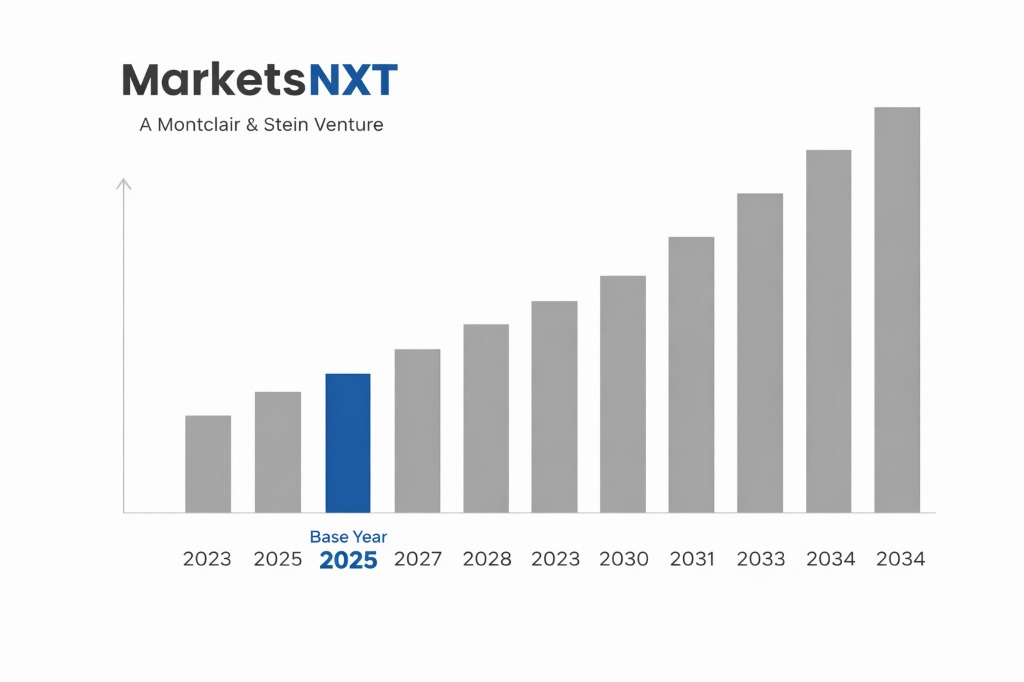
- ✓Base Year: 2025
- ✓Forecast Period: 2026–2032
Analyst Recommendation — Secure Pellicle Supply Now: Buyers and fab operators must qualify a second domestic pellicle supplier before Q3 2026. ASML's High-NA EUV rollout will double pellicle consumption per wafer layer, and current single-source dependency will cause yield-limiting delays at advanced nodes within 18 months.
South Korea's Role in the Global EUV Lithography Supply Chain
South Korea stands as the world's largest end-user of EUV lithography equipment, absorbing an estimated 35–40% of all ASML EUV scanner shipments annually. Samsung Electronics and SK Hynix collectively operate more than 80 EUV systems across fabs in Hwaseong, Pyeongtaek, and Icheon, processing sub-7nm logic and advanced DRAM at scale no other country matches. This demand concentration gives South Korea unmatched influence over ASML's production scheduling, tool configuration priorities, and service infrastructure deployment, effectively making Incheon Airport a critical node in the global EUV logistics network for machine components and spare parts.
South Korea is a net importer of EUV capital equipment — all scanners originate from ASML's Veldhoven facility in the Netherlands — but a significant domestic value-add ecosystem has developed around photomasks, photoresists, and process gases. Companies such as S&S Tech and Hynix-affiliated suppliers produce EUV-grade photomasks domestically, reducing import dependency for consumables. However, EUV-specific photoresist chemistry and high-purity pellicle membranes remain heavily import-dependent, sourced primarily from Japan's JSR, Sumitomo Chemical, and Shin-Etsu Chemical, exposing South Korean fabs to Japan-origin supply disruptions that resurfaced as a real risk during the 2019 export control dispute.
Growth Drivers for EUV Lithography Trade and Production in South Korea
The primary growth driver is Samsung Electronics' aggressive capacity expansion at its Pyeongtaek P4 and P5 mega-fabs, which are specifically designed to accommodate High-NA EUV systems alongside existing Low-NA tools. Samsung's foundry roadmap targets 2nm gate-all-around production by 2025, requiring additional EUV tool layers per chip — from approximately 14 layers at 5nm to over 20 layers at 2nm — directly multiplying EUV scanner procurement volumes and consumable throughput. South Korea's national semiconductor cluster strategy, backed by KRW 300 trillion in private investment commitments through 2047, underpins sustained capital equipment import demand for at least the next decade.
SK Hynix's transition from conventional DRAM to High Bandwidth Memory (HBM) at advanced nodes represents the second major driver, with each HBM3E die requiring EUV patterning at 1znm and below. SK Hynix's Icheon M16 fab and the new Yongin campus — planned at USD 87 billion over 20 years — will require successive EUV tool deliveries through 2032. A third driver is South Korea's government-backed import substitution program for EUV ancillary materials, injecting direct R&D subsidies into domestic photoresist and pellicle development through MOTIE-funded consortia, gradually reshaping the consumables trade balance from import-heavy toward partial domestic self-sufficiency by 2028.
Supply Chain Risks and Trade Barriers
The most acute supply chain risk facing South Korean EUV operations is the single-source dependency on ASML for scanner hardware, compounded by Dutch export licensing requirements that now extend to High-NA EUV systems under tightened Wassenaar-adjacent controls. Any geopolitical deterioration in Netherlands-Korea trade relations, or a Dutch regulatory shift mirroring US pressure on ASML, directly freezes capacity expansion timelines for both Samsung and SK Hynix. Lead times for EUV tools currently run 18–24 months, meaning any licensing disruption creates multi-year production gaps that competitors in Taiwan — specifically TSMC — would immediately exploit to capture advanced foundry market share.
Japan's export controls on fluorinated polyimide, hydrogen fluoride, and photoresist precursors — imposed in July 2019 — demonstrated that South Korea's EUV consumables supply chain carries unquantified Japan-origin concentration risk. Although bilateral relations have partially normalized since 2023, the structural dependency persists: over 70% of chemically amplified resists qualified for EUV patterning in Korean fabs are still Japanese-origin. Additionally, South Korea's logistics infrastructure for EUV components — specifically vibration-controlled specialized freight for optical module transport — relies on a narrow set of certified air cargo handlers at Incheon, creating capacity pinch points during simultaneous multi-fab tool installation campaigns.
Trade and Investment Opportunities in South Korea's EUV Market
The most commercially significant near-term opportunity is domestic EUV photoresist development and qualification, where South Korean chemical firms including Dongjin Semichem and Kolon Industries are advancing metal-oxide resist formulations that directly substitute for Japanese imports. Any supplier achieving full qualification at Samsung or SK Hynix before 2027 captures a recurring annual revenue stream estimated at USD 200–300 million per fab, given EUV resist consumption rates at high-volume manufacturing. International specialty chemical companies establishing joint ventures with Korean partners gain preferential access to fab qualification pipelines that are effectively closed to cold-approach foreign entrants operating without local presence.
Inbound foreign direct investment targeting EUV-adjacent infrastructure presents a second opportunity tier. ASML itself has expanded its Korean service and training center in Hwaseong, and component suppliers such as Carl Zeiss SMT and Trumpf — which supplies EUV light source laser systems — have established or are expanding Korean service entities to reduce tool downtime. The South Korean government's Foreign Investment Promotion Act offers tax exemptions up to five years for advanced semiconductor equipment service operations, making Korea an attractive regional hub for multinational EUV supply chain participants to base their Asia-Pacific technical operations rather than routing through Singapore or Japan.
Market at a Glance
| Metric | Detail |
|---|---|
| Market Size 2024 | USD 1.82 Billion |
| Market Size 2032 | USD 5.47 Billion |
| Growth Rate | 14.8% CAGR |
| Most Critical Decision Factor | ASML tool allocation and delivery lead time management |
| Largest End-User | Samsung Electronics |
| Competitive Structure | Monopolistic equipment supply; duopolistic domestic end-use |
Leading Market Participants
- ASML
- Samsung Electronics
- SK Hynix
- JSR Corporation
- Shin-Etsu Chemical
- Sumitomo Chemical
- S&S Tech
- Dongjin Semichem
- FST Co., Ltd.
- Trumpf
Regulatory and Trade Policy Environment
South Korea's EUV lithography trade operates within a complex multilateral framework anchored by the Korea-EU Free Trade Agreement, which sets zero tariffs on semiconductor capital equipment imports from the Netherlands, directly reducing ASML scanner procurement costs relative to non-FTA jurisdictions. The US-Korea bilateral investment framework and the CHIPS Act-era semiconductor alliance further shape procurement terms, as Korean fabs receiving US government incentives for overseas operations — including Samsung's Taylor, Texas facility — must navigate US export administration rules that increasingly govern re-export of EUV-processed wafers and derivative technologies. South Korea's own Strategic Goods Export Control Act mirrors Wassenaar controls on advanced semiconductor manufacturing equipment, restricting outbound transfer of EUV-related know-how to non-allied states.
Domestically, South Korea's Special Act on National Advanced Strategic Industries — enacted in 2022 — designates EUV-capable semiconductor fabrication as a nationally protected industrial activity, granting accelerated permitting, utility priority, and environmental regulation carve-outs for qualifying fab projects in the Yongin and Pyeongtaek semiconductor cluster zones. The act also mandates preferential procurement of domestically produced EUV consumables where technically equivalent options exist, directly incentivizing local photoresist and photomask suppliers. Import tariff exemptions under the Act's industrial equipment provisions apply to EUV scanners and their certified ancillary systems, effectively maintaining a zero-duty import cost structure for all ASML hardware entering South Korean fabs through 2032.
South Korea's EUV Lithography Supply Chain Outlook to 2032
South Korea's EUV supply chain position will shift materially toward higher domestic value-add between 2025 and 2032, driven by government-mandated localization targets for photoresist, pellicles, and photomask blanks under the Strategic Industries Act. Samsung's internal materials qualification roadmap targets 30% domestic sourcing for EUV consumables by 2028, up from under 15% in 2024. The introduction of High-NA EUV systems — with ASML's EXE:5000 platform first installed at Samsung Hwaseong in late 2024 — will reconfigure fab layouts, increase power infrastructure requirements, and demand new pellicle and reticle handling protocols that currently have no qualified domestic solution, temporarily increasing import intensity before localization catches up.
By 2032, South Korea's EUV ecosystem will evolve from a pure capital equipment importer to a partial supply chain originator, particularly in photomask and advanced resist segments. The Yongin Semiconductor Cluster, once operational at scale after 2027, will concentrate over 150 EUV-capable wafer starts per month across Samsung and SK Hynix operations, cementing South Korea's position as the world's highest-density EUV manufacturing geography. However, the scanner hardware monopoly of ASML and the photochemical dependency on Japan will remain structural features of the supply chain through 2032, ensuring that South Korea's EUV ambitions remain subject to the trade policy decisions of its two most critical technology partners.
Market Segmentation
By Equipment Type
- Low-NA EUV Scanners
- High-NA EUV Scanners
- EUV Light Sources
- EUV Metrology and Inspection Tools
- Reticle Handling Systems
By Consumable Type
- EUV Photoresists
- EUV Photomasks
- Pellicles
- Photomask Blanks
- Process Gases
- Cleaning Chemicals
By Application Node
- 7nm and 5nm Logic
- 3nm and 2nm Logic
- Advanced DRAM (1z/1a/1b nm)
- High Bandwidth Memory
- NAND Flash Advanced Layers
By End-User
- Integrated Device Manufacturers
- Pure-Play Foundries
- Memory Manufacturers
- Research Institutes and Universities
Frequently Asked Questions
South Korea is 100% dependent on ASML for EUV scanner hardware, as no alternative manufacturer has achieved commercial EUV production capability. No credible alternative to ASML EUV scanners exists for sub-7nm patterning within the 2026–2032 forecast window.
EUV systems are disassembled into over 40 freight components at Veldhoven and transported via dedicated chartered cargo aircraft to Incheon International Airport, requiring vibration-isolated containers for optical modules. Final assembly and calibration at the fab site takes 3–6 months after delivery.
The 2019 controls forced Samsung and SK Hynix to accelerate domestic qualification of EUV photoresists and hydrogen fluoride alternatives, producing measurable supply chain diversification. However, Japanese-origin chemicals still account for over 70% of qualified EUV resist supply as of 2024.
The Korea-EU FTA eliminates import tariffs on semiconductor capital equipment from the Netherlands, directly reducing ASML scanner landed costs. The Special Act on National Advanced Strategic Industries further grants domestic fab operators import duty exemptions on EUV ancillary systems certified under the act.
High-NA EUV adoption increases per-tool power consumption by over 50% and requires entirely new pellicle chemistries with no currently qualified domestic South Korean supplier. This creates a temporary deepening of import dependency for pellicles and specialized optical components before localization programs can deliver qualified alternatives.
Frequently Asked Questions
Market Segmentation
- Low-NA EUV Scanners
- High-NA EUV Scanners
- EUV Light Sources
- EUV Metrology and Inspection Tools
- Reticle Handling Systems
- EUV Photoresists
- EUV Photomasks
- Pellicles
- Photomask Blanks
- Process Gases
- Cleaning Chemicals
- 7nm and 5nm Logic
- 3nm and 2nm Logic
- Advanced DRAM (1z/1a/1b nm)
- High Bandwidth Memory
- NAND Flash Advanced Layers
- Integrated Device Manufacturers
- Pure-Play Foundries
- Memory Manufacturers
- Research Institutes and Universities
Table of Contents
Research Framework and Methodological Approach
Information
Procurement
Information
Analysis
Market Formulation
& Validation
Overview of Our Research Process
MarketsNXT follows a structured, multi-stage research framework designed to ensure accuracy, reliability, and strategic relevance of every published study. Our methodology integrates globally accepted research standards with industry best practices in data collection, modeling, verification, and insight generation.
1. Data Acquisition Strategy
Robust data collection is the foundation of our analytical process. MarketsNXT employs a layered sourcing model.
- Company annual reports & SEC filings
- Industry association publications
- Technical journals & white papers
- Government databases (World Bank, OECD)
- Paid commercial databases
- KOL Interviews (CEOs, Marketing Heads)
- Surveys with industry participants
- Distributor & supplier discussions
- End-user feedback loops
- Questionnaires for gap analysis
Analytical Modeling and Insight Development
After collection, datasets are processed and interpreted using multiple analytical techniques to identify baseline market values, demand patterns, growth drivers, constraints, and opportunity clusters.
2. Market Estimation Techniques
MarketsNXT applies multiple estimation pathways to strengthen forecast accuracy.
Bottom-up Approach
Aggregating granular demand data from country level to derive global figures.
Top-down Approach
Breaking down the parent industry market to identify the target serviceable market.
Supply Chain Anchored Forecasting
MarketsNXT integrates value chain intelligence into its forecasting structure to ensure commercial realism and operational alignment.
Supply-Side Evaluation
Revenue and capacity estimates are developed through company financial reviews, product portfolio mapping, benchmarking of competitive positioning, and commercialization tracking.
3. Market Engineering & Validation
Market engineering involves the triangulation of data from multiple sources to minimize errors.
Extensive gathering of raw data.
Statistical regression & trend analysis.
Cross-verification with experts.
Publication of market study.
Client-Centric Research Delivery
MarketsNXT positions research delivery as a collaborative engagement rather than a static information transfer. Analysts work with clients to clarify objectives, interpret findings, and connect insights to strategic decisions.