South Korea Semiconductor Equipment Market Size, Share & Forecast 2026–2034
Report Highlights
- ✓Market Size 2024: Approximately USD 14.2 billion
- ✓Market Size 2034: Approximately USD 38.6 billion
- ✓CAGR Range: 10.5%–12.1%
- ✓Market Definition: Semiconductor fab equipment manufactured and deployed in South Korea, covering etch, deposition, lithography, and inspection systems.
- ✓Key Market Highlight: Korea's semiconductor equipment cluster — SEMES, Eugene Technology, and Jusung Engineering — supplies Samsung and SK Hynix with domestic alternatives to ASML, Applied Materials, and Lam Research, reducing US export control exposure for Korean fabs.
- ✓Top 5 Companies: ASML Korea (subsidiary), Applied Materials Korea, Lam Research Korea, Jusung Engineering, SFA Engineering
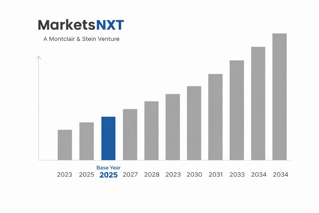
- ✓Base Year: 2025
- ✓Forecast Period: 2026–2034
- ✓Contrarian Insight: Korea's semiconductor equipment cluster — SEMES, Eugene Technology, and Jusung Engineering — supplies Samsung and SK Hynix with domestic alternatives to ASML, Applied Materials, and Lam Research, reducing US export control exposure for Korean fabs.
Industry Snapshot
The South Korea Semiconductor Equipment market was valued at approximately USD 14.2 billion in 2024 and is projected to reach approximately USD 38.6 billion by 2034, growing at a CAGR of 10.5%–12.1% over the forecast period. South Korea is the world's largest memory semiconductor producer — Samsung Electronics and SK Hynix together account for approximately 70% of global DRAM revenue and approximately 50% of NAND flash revenue — creating a captive equipment procurement base larger than any single country outside Taiwan. Equipment spending at Korean fabs follows a cyclical pattern driven by memory pricing cycles, but the structural trend is expansion: Samsung's USD 300 billion domestic semiconductor investment plan through 2042 and SK Hynix's Yongin semiconductor cluster (USD 90 billion through 2046) provide the strongest medium-term equipment demand anchors in the global semiconductor industry.
The competitive dynamics of the Korean equipment market are shaped by the tension between Samsung and SK Hynix's preference for globally proven equipment — particularly ASML's EUV lithography systems, Applied Materials' CVD and etch tools, and Lam Research's etch technology — and the Korean government's explicit policy goal of increasing domestic equipment supply to reduce geopolitical supply chain risk. Korean fabs currently source approximately 80%–85% of equipment value from non-Korean manufacturers, a concentration that became a policy concern following the 2019 Japan export controls on semiconductor materials and the subsequent recognition that equipment supply concentration carries analogous risk. The K-Semiconductor Belt strategy and its KRW 510 trillion (USD 450 billion) semiconductor ecosystem investment target explicitly funds domestic equipment supplier development through R&D subsidies, purchase guarantees at Korean fabs, and export credit support for Korean equipment makers entering global markets.
Competitive Intensity Assessment
Competition in South Korea's semiconductor equipment market operates across five dimensions with clear asymmetries. Active competitors: the global equipment market in Korea is dominated by five to seven international companies (ASML, Applied Materials, Lam Research, KLA, Tokyo Electron) for leading-edge nodes, with Korean domestic suppliers (Jusung Engineering, SFA Engineering, Eugene Technology, Wonik IPS) competing primarily in commodity deposition, thermal processing, and ALD equipment segments. Price competition: leading-edge equipment (EUV, high-NA EUV) is non-price-sensitive — Samsung and SK Hynix pay ASML's published EUV list price with no meaningful negotiation leverage due to ASML's monopoly position at leading lithography nodes; commodity equipment is moderately price-competitive with Korean domestic alternatives undercutting Japanese and US equivalents by 10%–25%. Product differentiation: extreme at leading-edge nodes where ASML's EUV is technically irreplaceable; moderate at etch and deposition where Applied Materials, Lam Research, and TEL compete on process integration advantage. Switching costs: the highest in any equipment category — fab process integration around specific equipment suppliers requires 18–36 months of re-qualification even for technically equivalent alternatives. Barriers to entry: extreme for EUV and advanced etch — Korean domestic entrants face 10–15 year technology development gaps for leading-edge equipment.
Three companies will most significantly reshape South Korean equipment market share through 2027. ASML's transition to high-NA EUV delivery — with Samsung receiving first high-NA EUV systems for 2nm process development in 2024 — creates a procurement cycle of 20–30 systems per year at EUR 300–400 million each, concentrating approximately EUR 6–10 billion of annual Korean fab equipment spending in a single supplier. SK Hynix's HBM3E capacity expansion — targeting 60% global HBM market share — requires hybrid bonding and advanced packaging equipment where domestically developed suppliers (Hanmi Semiconductor) are gaining qualification, representing the most significant Korean domestic equipment market share gain opportunity. Applied Materials' introduction of Vistara chip manufacturing platform — integrating etch, deposition, and annealing in a unified architecture — is reshaping Samsung's advanced logic fab equipment qualification decisions in a direction that benefits integrated platform providers over single-process-step specialists.
Market Growth Drivers
HBM (High Bandwidth Memory) demand driven by AI GPU deployment is the single most important near-term demand driver for Korean semiconductor equipment. SK Hynix's monopoly on HBM3E qualification at NVIDIA — supplying approximately 70% of H100 and H200 GPU HBM3E memory — requires sustained capacity expansion that drives HBM-specific equipment procurement including thermal compression bonding systems (Hanmi Semiconductor), advanced CMP, and through-silicon via (TSV) equipment. Samsung's foundry business expansion at its Taylor, Texas fabrication facility (USD 17 billion investment) creates equipment procurement that, while physically located in the US, is managed by Korean semiconductor engineers and often procured through Korean equipment subsidiaries — maintaining Korean market relevance for US fab equipment decisions. The global DRAM market recovery — with DRAM ASPs recovering approximately 50%–70% from 2023 trough levels driven by AI server demand — restored equipment procurement budgets at Samsung and SK Hynix that were sharply curtailed in 2023, with equipment spending projected to return to peak 2021–2022 levels by 2025–2026.
The K-Semiconductor Belt strategy's purchase guarantee mechanism is a supply-push driver for domestic equipment suppliers. Korean fabs receive tax credits for purchasing domestically manufactured semiconductor equipment, and MOTIE (Ministry of Trade, Industry and Energy) administers a domestic equipment evaluation programme where Samsung and SK Hynix are incentivised to evaluate and qualify Korean equipment alternatives even where global alternatives are proven. Jusung Engineering's ALD equipment qualification at Samsung for 3nm GAAFET gate oxide deposition and Wonik IPS's thermal processing equipment expansion at SK Hynix represent the concrete market share gains that this policy mechanism is generating for Korean domestic suppliers.
Market Restraints and Challenges
EUV system availability constraints impose the most significant supply-side ceiling on Korean fab capacity expansion timelines. ASML manufactures approximately 40–55 EUV systems annually — limited by Carl Zeiss SMT optics production and tin plasma light source engineering — with allocation distributed across TSMC, Samsung, Intel, and SK Hynix globally. Samsung currently receives approximately 10–15 EUV systems per year, and its leading-edge logic and DRAM process roadmaps require EUV at gate-all-around (GAAFET) 3nm and DRAM 1a/1b nodes — creating a dependency on ASML's constrained production that cannot be resolved through procurement negotiation. High-NA EUV production capacity is similarly constrained — ASML is targeting 20 high-NA EUV systems annually by 2025–2026, with Samsung and SK Hynix competing with TSMC and Intel for allocation.
Geopolitical risk cuts in both directions for Korean semiconductor equipment. US export controls on advanced semiconductor equipment to China — while currently providing Korean fabs with ASML, Applied Materials, and Lam Research supply chain preferential positioning — introduce the risk that future US semiconductor policy could restrict certain equipment supply to Korean fabs as well if Korean fabs are found to violate end-use controls. Samsung and SK Hynix each maintain Chinese fab operations (Samsung Xian NAND, SK Hynix Wuxi DRAM and Dalian NAND) where equipment upgrade restrictions are already applied under current BIS rules, creating operational complexity and productivity constraints at Chinese fabs that indirectly affect Korean equipment market size by reducing effective equipment deployment opportunities.
Emerging Opportunities
Advanced packaging equipment — specifically hybrid bonding, fan-out wafer-level packaging (FOWLP), and high-density interconnect systems — is the fastest-growing Korean equipment segment, driven by HBM, chiplet integration, and AI SoC packaging requirements. Hanmi Semiconductor, the leading Korean advanced packaging equipment supplier, has seen revenue grow approximately 3x between 2022 and 2024 driven by HBM thermal compression bonding system orders — a trajectory projected to continue as HBM4 and HBM4E generation require even tighter bonding pitch tolerances. Korean metrology and inspection equipment — Onto Innovation Korea, Nanometrics Korea, and domestic developers including Inspekto and Onto — benefit from the increasing inspection intensity at advanced nodes where defect density requirements tighten at each lithography generation.
Regulatory and Policy Landscape
The K-Semiconductor Belt Strategy (2021) and the Semiconductor Industry Competitiveness Enhancement Special Act (proposed 2023) define the Korean policy framework — combining investment tax credits (25% for fab investment, 15% for R&D), domestic equipment purchase incentives, and infrastructure support for the Yongin semiconductor cluster. MOTIE administers equipment localisation programmes through the Semiconductor Equipment and Materials Development Programme. The Korean trade ministry coordinates with BIS on US export control implementation to ensure Korean fab operations have clarity on equipment upgrade permissions at their Chinese facilities — a diplomatically sensitive ongoing engagement.
Leading Market Participants
- ASML Korea
- Applied Materials Korea
- Lam Research Korea
- Tokyo Electron Korea (TEL)
- KLA Korea
- Jusung Engineering
- SFA Engineering
- Hanmi Semiconductor
- Wonik IPS
- Eugene Technology
Domestic vs. International Dynamics
International equipment suppliers — primarily ASML, Applied Materials, Lam Research, TEL, and KLA — account for approximately 80%–85% of Korean semiconductor equipment spending by value, concentrated in leading-edge lithography, etch, deposition, and metrology where Korean domestic alternatives are not yet qualified at advanced nodes. International players have structural advantages in Korea: global reference fabs (TSMC, Intel) provide process integration data that Korean fab engineers trust; global service networks provide 24/7 support at the speed Korean fab productivity requirements demand; and US export control treatment gives US equipment suppliers a privileged supply relationship with Korean fab operations that could be jeopardised if Korean fabs sourced significant equipment from non-allied suppliers. Korean domestic equipment suppliers — Jusung, SFA, Wonik IPS, Hanmi — currently hold 15%–20% of equipment market value, concentrated in ALD, thermal processing, substrate handling, and advanced packaging segments below the leading-edge lithography and etch tiers.
The domestic-international balance is shifting toward domestic suppliers under the K-Semiconductor Belt policy pressure, with the government target of 30%+ domestic equipment share by 2030 providing explicit market share targets that Korean fabs are incentivised to support. The most credible domestic market share gains through 2027 are in advanced packaging equipment (Hanmi Semiconductor leading), ALD equipment (Jusung Engineering and Eugene Technology with Samsung qualifications), and semiconductor substrate and carrier handling automation (SFA Engineering). The technology gap at EUV lithography and leading-edge etch remains a 10–15 year development challenge that policy incentives alone cannot close — making the 30% domestic share target achievable only if packaging equipment gains are substantially counted in the total equipment value base.
Long-Term Market Perspective
South Korea's semiconductor equipment market through 2034 will grow from USD 14.2 billion to USD 38.6 billion driven by Samsung's Yongin cluster phased activation, SK Hynix's HBM and DRAM next-generation capacity, and Samsung Foundry's domestic advanced logic capacity expansion. The domestic equipment supply share will expand from 15%–20% toward 25%–30% by 2034 under policy pressure and in packaging equipment specifically, but will remain below the government's 30% aggregate target due to continued international supplier dominance in lithography and etch. The geopolitical tailwind from US export controls diverting ASML and US equipment away from Chinese fabs toward Korean fabs provides a structural procurement advantage that is expected to persist through the 2034 forecast period, reinforcing Korea's equipment vendor relationships and allocation priority.
The most significant risk to the 2034 trajectory is a technology disruption at the lithography layer — if TSMC gains a decisive EUV process advantage over Samsung in leading-edge logic while Samsung's foundry faces yield and customer acquisition challenges, Samsung's foundry capex could be curtailed, reducing equipment demand from the foundry sector below projections. Memory equipment demand is more structurally resilient — AI infrastructure build-out creates a decade-long HBM demand anchor that is less dependent on Samsung's competitive position than the foundry equipment cycle.
Frequently Asked Questions
Market Segmentation
- Lithography Systems (EUV and DUV)
- Etch and Deposition Equipment
- Advanced Packaging Equipment (Hybrid Bonding, TSV, FOWLP)
- Others (CMP, Ion Implant, Metrology and Inspection)
- DRAM Memory Fabrication
- NAND Flash Memory Fabrication
- HBM and Advanced Memory Packaging
- Logic Foundry and System-on-Chip Fabrication
- Power Semiconductor and Compound Semiconductor Fabrication
- Direct OEM Equipment Sales to Samsung and SK Hynix
- Korean Equipment Subsidiary Operations
- MOTIE Domestic Equipment Programme Procurement
- OSAT and Packaging Contractor Procurement
Table of Contents
Research Framework and Methodological Approach
Information
Procurement
Information
Analysis
Market Formulation
& Validation
Overview of Our Research Process
MarketsNXT follows a structured, multi-stage research framework designed to ensure accuracy, reliability, and strategic relevance of every published study. Our methodology integrates globally accepted research standards with industry best practices in data collection, modeling, verification, and insight generation.
1. Data Acquisition Strategy
Robust data collection is the foundation of our analytical process. MarketsNXT employs a layered sourcing model.
- Company annual reports & SEC filings
- Industry association publications
- Technical journals & white papers
- Government databases (World Bank, OECD)
- Paid commercial databases
- KOL Interviews (CEOs, Marketing Heads)
- Surveys with industry participants
- Distributor & supplier discussions
- End-user feedback loops
- Questionnaires for gap analysis
Analytical Modeling and Insight Development
After collection, datasets are processed and interpreted using multiple analytical techniques to identify baseline market values, demand patterns, growth drivers, constraints, and opportunity clusters.
2. Market Estimation Techniques
MarketsNXT applies multiple estimation pathways to strengthen forecast accuracy.
Bottom-up Approach
Aggregating granular demand data from country level to derive global figures.
Top-down Approach
Breaking down the parent industry market to identify the target serviceable market.
Supply Chain Anchored Forecasting
MarketsNXT integrates value chain intelligence into its forecasting structure to ensure commercial realism and operational alignment.
Supply-Side Evaluation
Revenue and capacity estimates are developed through company financial reviews, product portfolio mapping, benchmarking of competitive positioning, and commercialization tracking.
3. Market Engineering & Validation
Market engineering involves the triangulation of data from multiple sources to minimize errors.
Extensive gathering of raw data.
Statistical regression & trend analysis.
Cross-verification with experts.
Publication of market study.
Client-Centric Research Delivery
MarketsNXT positions research delivery as a collaborative engagement rather than a static information transfer. Analysts work with clients to clarify objectives, interpret findings, and connect insights to strategic decisions.