Taiwan Advanced Semiconductor Market Size, Share & Forecast 2026–2034
Report Highlights
- ✓Market Size 2024: Approximately USD 142.6 billion
- ✓Market Size 2034: Approximately USD 412.8 billion
- ✓CAGR Range: 11.2%–12.6%
- ✓Market Definition: Advanced logic and memory semiconductor fabrication in Taiwan, led by TSMC, UMC, and MediaTek across sub-7nm nodes through 2N processes.
- ✓Key Market Highlight: TSMC controls ~92% of global sub-10nm foundry capacity — Taiwan's concentration of advanced semiconductor IP, talent, and infrastructure represents the most strategically important single-nation technology concentration in the global economy.
- ✓Top 5 Companies: TSMC, MediaTek, ASE Technology Holding, Novatek Microelectronics, Realtek Semiconductor
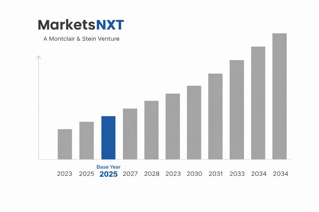
- ✓Base Year: 2025
- ✓Forecast Period: 2026–2034
- ✓Contrarian Insight: TSMC controls ~92% of global sub-10nm foundry capacity — Taiwan's concentration of advanced semiconductor IP, talent, and infrastructure represents the most strategically important single-nation technology concentration in the global economy.
Industry Snapshot
The Taiwan Advanced Semiconductor market was valued at approximately USD 142.6 billion in 2024 and is projected to reach approximately USD 412.8 billion by 2034, growing at a CAGR of 11.2%–12.6% over the forecast period. Taiwan produces approximately 65%–70% of the world's semiconductor chips by value and approximately 90% of leading-edge (sub-7nm) logic chips — a concentration with no historical parallel in critical global manufacturing. TSMC alone accounts for approximately 60% of global foundry revenue and 90%+ of sub-5nm capacity. The Taiwan semiconductor ecosystem — TSMC as foundry anchor, ASML-supplied EUV lithography, domestic equipment and materials suppliers (ASE, King Yuan Electronics, Globalink), and a dense fabless IC design sector — creates interlocking competitive advantages that have proven extraordinarily difficult to replicate at comparable cost, scale, and technical capability.
The competitive landscape is defined by TSMC's structural position and the IC design sector's global customer base. TSMC's N3 (3nm class) process entered high-volume manufacturing in 2023 serving Apple (A17 Pro, M3), NVIDIA, and AMD — with N2 (2nm equivalent gate-all-around) targeted for 2025 and A16 (sub-2nm, backside power delivery) for 2026. No other foundry has demonstrated N3-equivalent in production; Intel Foundry Services' 18A (1.8nm) is targeted for 2025 but has not yet entered volume production. Samsung Foundry's 3nm GAA entered limited production in 2022 but yield and customer adoption have lagged TSMC significantly. MediaTek — Taiwan's largest fabless IC design company and second-largest global fabless designer — designs smartphone SoCs, Wi-Fi chips, and AI inference accelerators consumed by Chinese, European, and global OEMs, with annual revenues exceeding USD 17 billion and customer concentration across Samsung, Xiaomi, and Oppo.
Competitive Intensity Assessment
Taiwan's advanced semiconductor market competes across five dimensions. Active competitors: at the foundry layer, effective competition is TSMC versus two credible but trailing alternatives (Samsung Foundry, Intel IFS) — Taiwan-versus-Taiwan competition is absent since TSMC is the sole advanced foundry in Taiwan. At the IC design layer, Taiwan hosts approximately 250 active fabless design houses competing globally in mobile, networking, display, and storage chip segments. Price competition: TSMC commands 20%–30% pricing premiums over Samsung Foundry for equivalent node specifications based on superior yield and customer confidence — indicating pricing power that reflects genuine performance differentiation rather than oligopolistic behaviour. Product differentiation: TSMC differentiates through leading-edge node delivery schedule (consistently first to sub-7nm volume production), CoWoS and SoIC 3D packaging, and dedicated advanced technology centres co-developing with NVIDIA, Apple, and AMD. Switching costs: foundry switching requires 6–18 months of process migration and yield qualification at the new node — significant but not prohibitive for mature nodes; at leading-edge, TSMC's proprietary N3P and N2 chemistry create practical barriers that make switching functionally infeasible mid-product-generation. Barriers to entry: extreme — leading-edge foundry requires USD 20–30 billion capital per fab, ASML EUV scanner allocation (limited to 50–60 units globally per year), and 5–10 year process development investment.
Three companies will most significantly reshape Taiwan's competitive position through 2027. Apple — accounting for approximately 25% of TSMC revenue — is expanding its custom silicon programme to include server AI chips (Project ACDC), modem chips (replacing Qualcomm in iPhones), and display driver ICs, deepening its Taiwan supply chain dependency while concentrating TSMC revenue at a level that creates single-customer concentration risk. NVIDIA — TSMC's second-largest customer — is consuming the majority of TSMC's CoWoS advanced packaging capacity for H100/H200/B200 GPUs, driving TSMC's most aggressive capacity investment cycle and generating the pricing power that makes TSMC's 2024–2025 capex of USD 32–36 billion the largest in corporate history. Intel Foundry Services — seeking to leverage Intel 18A technology to reclaim process leadership from TSMC — represents the first genuine competitive technology threat to TSMC's leading-edge position since 2015, though commercial customer adoption of IFS 18A at volume scale has not yet been demonstrated.
Market Growth Drivers
AI chip demand is the dominant near-term driver, consuming TSMC's most advanced capacity and generating the volume and pricing that underpin TSMC's 2024–2026 capital investment cycle. NVIDIA's GB200 NVL72 (Blackwell architecture, TSMC N4P process, CoWoS-L packaging) and Apple's M4 chip (TSMC N3E) represent the primary near-term demand anchors for TSMC's most advanced capacity. Hyperscaler ASIC demand — Google TPU v5, Amazon Trainium2, Microsoft Maia — provides additional leading-edge N3/N2 demand with multi-year committed volumes that stabilise TSMC's capex return timeline. Taiwan's IC design sector benefits disproportionately from AI chip demand: MediaTek's Dimensity AI NPU in premium smartphones, Novatek's AI display driver chips, and Realtek's AI-enhanced networking chips all represent AI-driven product cycles expanding addressable markets for Taiwanese fabless designers.
Advanced packaging technology development is a second structural growth driver. TSMC's CoWoS (Chip-on-Wafer-on-Substrate) and SoIC (System-on-Integrated-Chips) 3D stacking technologies are enabling chiplet integration at the boundary of what monolithic die scaling achieves, extending the value of TSMC's customer relationships beyond wafer fabrication into the advanced packaging layer previously served by ASE Group and Amkor. TSMC's CoWoS capacity — targeted at 50,000 wpm by end 2025 from approximately 15,000 wpm in 2023 — is the single most capacity-constrained step in the AI chip supply chain, giving TSMC effective control over the AI GPU production rate that drives the entire AI hardware investment cycle.
Market Restraints and Challenges
Geopolitical risk is the defining structural challenge. Cross-strait tension between Taiwan and China — China's assertion of sovereignty over Taiwan and periodic military escalation including August 2022 live-fire military exercises encircling Taiwan — creates a systemic risk premium for the entire global semiconductor supply chain dependent on Taiwan. TSMC's international diversification programme (TSMC Arizona N4/N3, TSMC Japan, TSMC Germany) is a partial response — but Arizona and Japan together will represent approximately 20%–25% of TSMC's advanced node capacity by 2030, leaving the global semiconductor supply chain highly Taiwan-dependent through the decade. The risk is asymmetric: Taiwan disruption would simultaneously eliminate 65%–70% of global chip production value and 90%+ of sub-5nm capacity, causing a global technology industry shutdown with no 12–24 month recovery pathway.
Talent competition and cost escalation are operational constraints. Taiwan's advanced semiconductor industry employs approximately 300,000 engineers and technicians — a labour pool that has historically been cost-competitive but is facing wage inflation as TSMC, UMC, GlobalFoundries Taiwan, and the IC design sector compete for limited STEM graduate supply. Engineering salaries at TSMC rose approximately 15%–20% between 2021 and 2024, compressing the labour cost advantage relative to Korean and US peers. TSMC's Arizona facility has encountered productivity gaps versus Taiwan operations attributed partly to workforce culture, training, and process knowledge transfer challenges — indicating that Taiwan's semiconductor advantage is partly non-transferable human capital that does not follow equipment and process documentation to new geographies.
Emerging Opportunities
Gate-all-around (GAA) transistor architecture transition at N2 (2nm equivalent) represents the next generational technology step — TSMC's N2 nanosheet GAA process entering volume production in 2025 for Apple A19 and next-generation AI inference chips will define the leading-edge competitive landscape for 2025–2027. Taiwan's materials and equipment ecosystem — including United Microelectronics Corporation (UMC) specialty process leadership in embedded memory and RF chips, and King Yuan Electronics' advanced test services — provides structural depth beyond TSMC that sustains Taiwan's ecosystem advantage through technology transitions. Silicon photonics integration — combining optical interconnects with advanced CMOS logic for AI data centre chip-to-chip communication at bandwidth and energy efficiency levels unachievable with copper — is an emerging segment where TSMC's COUPE (silicon photonics) process and Taiwan's optical component manufacturing base (Foxconn, Lumentum Taiwan) create genuine ecosystem advantages.
Regulatory and Policy Landscape
Taiwan's semiconductor industry operates under a supportive regulatory framework managed by the Ministry of Economic Affairs (MOEA) and the Industrial Development Bureau (IDB). The Statute for Industrial Innovation provides R&D tax credits of 15%–25% for qualifying semiconductor process development expenditures. Taiwan's export control regime — administered by the Bureau of Foreign Trade — aligns with US Export Administration Regulations for advanced semiconductor equipment and technology, providing strategic alignment with US tech export policy while maintaining Taiwan's commercial relationships with Chinese customers at below-leading-edge nodes (N7 and above). MOEA's semiconductor cluster development policy — sustaining the Hsinchu Science Park and Taichung and Tainan Science Parks as integrated R&D, fabrication, and OSAT ecosystems — provides industrial zoning, infrastructure, and utilities at terms that reduce new facility development cost by 20%–30% relative to greenfield industrial development.
Leading Market Participants
- TSMC (Taiwan Semiconductor Manufacturing Company)
- MediaTek
- ASE Technology Holding
- Novatek Microelectronics
- Realtek Semiconductor
- United Microelectronics Corporation (UMC)
- Phison Electronics
- King Yuan Electronics
- Powerchip Semiconductor Manufacturing (PSMC)
- Silicon Motion Technology
Domestic vs. International Dynamics
Taiwan-headquartered companies design and manufacture essentially 100% of the revenue generated in Taiwan's semiconductor industry — there is no meaningful foreign foundry or IC design presence within Taiwan itself. The international revenue dimension is the critical variable: TSMC generates approximately 60%+ of revenue from US-headquartered customers (Apple, NVIDIA, AMD, Qualcomm, Broadcom), approximately 10%–12% from Asian customers outside Taiwan, and approximately 7%–9% from European customers. MediaTek generates approximately 60%–65% of revenue from Chinese smartphone OEM customers — a customer concentration that creates US export control and BIS restriction exposure risk as semiconductor supply chain decoupling advances. Taiwan's semiconductor companies are structurally US-customer-dependent at the technology frontier (TSMC, advanced packaging) and China-customer-dependent at the volume application layer (MediaTek mobile, Novatek display).
The balance is shifting in favour of geographic diversification pressure from multiple directions simultaneously. TSMC is investing USD 65 billion in Arizona to meet US CHIPS Act requirements and customer supply chain security demands. MediaTek is diversifying customer base toward Indian, Latin American, and Southeast Asian smartphone OEMs to reduce China revenue concentration risk. ASE Group is establishing advanced packaging capacity in Malaysia and Arizona to serve customers requiring non-Taiwan supply chain options. The pace of this shift is constrained by the non-transferability of Taiwan's integrated ecosystem — relocating a single company creates a supply chain gap that weakens the argument for relocation, and the ecosystem advantage is preserved only if the majority of participants remain in Taiwan. This creates a structural equilibrium where incremental international diversification occurs without fundamental migration of the Taiwan semiconductor core.
Long-Term Market Perspective
Taiwan's advanced semiconductor market will reach USD 412.8 billion by 2034, anchored by TSMC's technology leadership extending to A16 and beyond, MediaTek's AI chip and automotive semiconductor product cycles, and advanced packaging's growing share of semiconductor value creation. The most significant structural development through 2034 is the extension of 3D chip stacking — heterogeneous integration of logic, memory, and photonics in a single package — from the current AI GPU application to commodity data centre, automotive, and consumer device applications, multiplying TSMC's value capture per wafer processed. Taiwan's challenge is sustaining the talent pipeline, research ecosystem, and infrastructure investment intensity required to maintain 2–3 generation process leadership as the human capital and capital requirements per technology generation increase exponentially.
The competitive dynamic most likely to reshape market structure is Intel Foundry Services' potential breakthrough to volume leading-edge production at Intel 18A or 14A. If IFS achieves N3-competitive yield at scale by 2026–2027, it would provide hyperscalers and fabless designers their first credible TSMC alternative for leading-edge AI and smartphone chip production — reducing TSMC's pricing power and shifting bargaining dynamics in customer relationships. Current assessment gives this scenario 20%–25% probability within the 2026–2028 window. The more likely scenario — IFS technical maturation taking until 2028–2030 — maintains TSMC's pricing power and Taiwan's structural market position through the majority of the forecast period.
Frequently Asked Questions
Market Segmentation
- Advanced Logic Foundry Services (Sub-7nm Node)
- IC Design and Fabless Semiconductor Products
- Advanced Packaging and OSAT Services
- Others (Specialty Processes, MEMS, Power Semiconductors)
- AI Data Centre and Hyperscale Computing
- Smartphone and Consumer Electronics
- Automotive and Industrial Semiconductors
- Networking and Communications Infrastructure
- Government and Defence Electronics
- Direct OEM Foundry Service Agreements
- Fabless-to-Foundry Design-In Pipeline
- OSAT and Packaging Service Contracts
- Distribution and Value-Added Reseller Channel
Table of Contents
Research Framework and Methodological Approach
Information
Procurement
Information
Analysis
Market Formulation
& Validation
Overview of Our Research Process
MarketsNXT follows a structured, multi-stage research framework designed to ensure accuracy, reliability, and strategic relevance of every published study. Our methodology integrates globally accepted research standards with industry best practices in data collection, modeling, verification, and insight generation.
1. Data Acquisition Strategy
Robust data collection is the foundation of our analytical process. MarketsNXT employs a layered sourcing model.
- Company annual reports & SEC filings
- Industry association publications
- Technical journals & white papers
- Government databases (World Bank, OECD)
- Paid commercial databases
- KOL Interviews (CEOs, Marketing Heads)
- Surveys with industry participants
- Distributor & supplier discussions
- End-user feedback loops
- Questionnaires for gap analysis
Analytical Modeling and Insight Development
After collection, datasets are processed and interpreted using multiple analytical techniques to identify baseline market values, demand patterns, growth drivers, constraints, and opportunity clusters.
2. Market Estimation Techniques
MarketsNXT applies multiple estimation pathways to strengthen forecast accuracy.
Bottom-up Approach
Aggregating granular demand data from country level to derive global figures.
Top-down Approach
Breaking down the parent industry market to identify the target serviceable market.
Supply Chain Anchored Forecasting
MarketsNXT integrates value chain intelligence into its forecasting structure to ensure commercial realism and operational alignment.
Supply-Side Evaluation
Revenue and capacity estimates are developed through company financial reviews, product portfolio mapping, benchmarking of competitive positioning, and commercialization tracking.
3. Market Engineering & Validation
Market engineering involves the triangulation of data from multiple sources to minimize errors.
Extensive gathering of raw data.
Statistical regression & trend analysis.
Cross-verification with experts.
Publication of market study.
Client-Centric Research Delivery
MarketsNXT positions research delivery as a collaborative engagement rather than a static information transfer. Analysts work with clients to clarify objectives, interpret findings, and connect insights to strategic decisions.