Taiwan AI Semiconductor Packaging and Advanced Node Market Size, Share & Forecast 2026–2034
Report Highlights
- ✓Country: Taiwan
- ✓Market: AI Semiconductor Packaging and Advanced Node Market
- ✓Market Size 2024: USD 16.6 billion
- ✓Market Size 2032: USD 74.3 billion
- ✓CAGR: 22.6%
- ✓Market Definition: Advanced semiconductor packaging (CoWoS, SoIC, FOWLP), extreme ultraviolet lithography fabrication at 3nm and below, and AI chip design and supply chain services in Taiwan.
- ✓Leading Companies: TSMC, ASE Technology, Amkor Technology Taiwan, KYEC, MediaTek
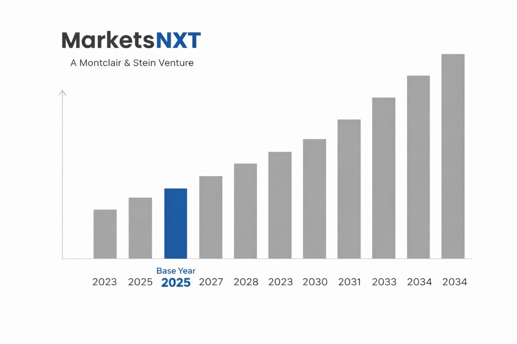
- ✓Base Year: 2025
- ✓Forecast Period: 2026–2032
Market Overview
Taiwan is the world's most critical single point in the AI semiconductor supply chain — a characterisation that industry, government, and geopolitical analysts have been making with increasing urgency since Nvidia's H100 GPU established the centrality of TSMC's advanced fabrication to AI compute infrastructure. TSMC manufactures approximately 90% of the world's most advanced logic semiconductors (3nm and below), including virtually every AI training chip of significance: Nvidia's H100, H200, and Blackwell GPUs, Google's TPU v4/v5, Apple's M4 chip, AMD's MI300X, and every custom AI accelerator designed by the major hyperscalers (Amazon Trainium, Microsoft Maia, Meta MTIA). The concentration of this fabrication capability in a geography of 36,000 km² — separated from mainland China by a 180 km strait — is the single most debated supply chain vulnerability in global technology.
Taiwan's semiconductor ecosystem extends beyond TSMC to a complete supply chain cluster: ASML EUV lithography systems (serviced in Taiwan), silicon wafer suppliers (GlobalWafers), photomask manufacturers (Photronics Taiwan), chemical suppliers (Eternal Materials, Chang Chun Group), OSAT (outsourced semiconductor assembly and test) companies (ASE Technology — the world's largest OSAT, Amkor Technology Taiwan, KYEC), and fabless design companies (MediaTek — the world's largest fabless chip designer by revenue in 2024). This cluster density means that a chip can progress from design tape-out to packaged tested die within Taiwan's semiconductor corridor (Hsinchu-Taichung-Tainan) with lead times and intellectual property security that geographically dispersed supply chains cannot match.
Key Growth Drivers
AI accelerator demand is TSMC's most powerful near-term growth driver — Nvidia's Blackwell GPU revenue run rate exceeded USD 100 billion annualised in early 2025, with TSMC capturing the foundry margin on every unit. The AI compute buildout of 2024–2028 is projected to require 5× growth in advanced semiconductor capacity relative to 2022 levels, and TSMC's capital expenditure programme (USD 30–35 billion annually) is the supply-side response to this demand signal. CoWoS (Chip on Wafer on Substrate) advanced packaging — TSMC's proprietary process for integrating AI chips with HBM memory in a single package — has been supply-constrained since 2023 with lead times of 12–18 months, driven by AI chip demand exceeding CoWoS capacity faster than TSMC can build it. Taiwan's advanced packaging revenue is the fastest-growing segment within its semiconductor value chain, growing at 35%+ annually.
Market Challenges
Geopolitical risk — specifically the possibility of Chinese military action affecting Taiwan's semiconductor manufacturing — is the existential market concern that has defined Taiwan semiconductor policy since 2022. US CHIPS Act investments in TSMC Arizona (2nm fab, 2028 target), Intel foundry development, and Samsung US expansion are explicit supply chain diversification responses, but none of these projects can replicate TSMC Taiwan's full capabilities within the 2025–2030 timeframe relevant to AI compute infrastructure. TSMC's Arizona fabs face 30%–40% higher production costs than Taiwan operations, workforce qualification challenges, and equipment lead times that will keep them behind Taiwan's technology frontier for years. The geopolitical risk is unquantifiable and uninsurable — it represents the market's most important non-commercial variable and justifies the CHIPS Act's USD 52 billion investment in semiconductor domestic capacity despite unfavourable economics versus Taiwan production.
Emerging Opportunities
TSMC's 2nm GAA process (expected commercial production 2025) and 1.4nm A14 process (development stage) represent the next frontier of AI chip performance that will maintain Taiwan's technology leadership for the remainder of the decade. The co-packaged optics opportunity — integrating photonic and electronic chips in the same package for AI datacentre optical I/O — is an emerging advanced packaging application where TSMC's SoIC (System on Integrated Chips) technology creates the integration density that AI switch ASICs require. Taiwan's semiconductor equipment ecosystem — ASML EUV servicing, Applied Materials, Lam Research, and KLA Tencor Taiwan operations — creates a local advanced process development capability that offshore TSMC fabs cannot replicate at equivalent productivity until the service infrastructure migrates with production.
Market at a Glance
| Parameter | Details |
|---|---|
| Market Size 2024 | USD 16.6 billion |
| Market Size 2032 | USD 74.3 billion |
| Growth Rate | 22.6% CAGR (2026–2032) |
| Most Critical Decision Factor | Technology maturity and regulatory readiness |
| Largest Segment | Largest domestic segment |
| Competitive Structure | Fragmented — multiple platform and specialist players |
Leading Market Participants
- ASE Technology is the world
- MediaTek
- KYEC and ChipMOS Technologies are Taiwan
- Novatek
- Realtek
Regulatory and Policy Environment
Taiwan's semiconductor policy is directed by the Industrial Development Administration's semiconductor cluster programme and ITRI (Industrial Technology Research Institute) technology development investment. Export control compliance with US BIS regulations — including licensing requirements for advanced chip exports to China — is a major operational consideration for TSMC, ASE, and other Taiwan semiconductor companies that must navigate US technology policy as the largest technology compliance issue in their industries. The Taiwan Semiconductor Industry Association (TSIA) coordinates industry engagement with government on export controls, CHIPS Act cooperation, and R&D investment programmes. TSMC's listing on NYSE (through ADRs) and its US customer concentration create transparency and accountability requirements that align the company's governance with US regulatory expectations in ways that domestically-listed Asian competitors do not face.
Long-Term Outlook
Taiwan's semiconductor market will grow at above-global-average rates through 2032, driven by AI chip demand that has structural rather than cyclical characteristics — AI infrastructure investment is compounding, not cycling, as foundation model capability growth drives continued compute investment. TSMC's 2nm production ramp and CoWoS capacity expansion will be the most commercially significant events in the 2025–2027 period. The long-term risk is not technology obsolescence — Taiwan's fabrication leadership is likely to persist through the decade — but geopolitical event risk that cannot be priced, hedged, or eliminated through supply chain investment. Taiwan's semiconductor industry is the most economically valuable and geopolitically consequential in history, and its trajectory through 2032 will shape the AI compute infrastructure of the global economy.
Frequently Asked Questions
Market Segmentation
Table of Contents
Research Framework and Methodological Approach
Information
Procurement
Information
Analysis
Market Formulation
& Validation
Overview of Our Research Process
MarketsNXT follows a structured, multi-stage research framework designed to ensure accuracy, reliability, and strategic relevance of every published study. Our methodology integrates globally accepted research standards with industry best practices in data collection, modeling, verification, and insight generation.
1. Data Acquisition Strategy
Robust data collection is the foundation of our analytical process. MarketsNXT employs a layered sourcing model.
- Company annual reports & SEC filings
- Industry association publications
- Technical journals & white papers
- Government databases (World Bank, OECD)
- Paid commercial databases
- KOL Interviews (CEOs, Marketing Heads)
- Surveys with industry participants
- Distributor & supplier discussions
- End-user feedback loops
- Questionnaires for gap analysis
Analytical Modeling and Insight Development
After collection, datasets are processed and interpreted using multiple analytical techniques to identify baseline market values, demand patterns, growth drivers, constraints, and opportunity clusters.
2. Market Estimation Techniques
MarketsNXT applies multiple estimation pathways to strengthen forecast accuracy.
Bottom-up Approach
Aggregating granular demand data from country level to derive global figures.
Top-down Approach
Breaking down the parent industry market to identify the target serviceable market.
Supply Chain Anchored Forecasting
MarketsNXT integrates value chain intelligence into its forecasting structure to ensure commercial realism and operational alignment.
Supply-Side Evaluation
Revenue and capacity estimates are developed through company financial reviews, product portfolio mapping, benchmarking of competitive positioning, and commercialization tracking.
3. Market Engineering & Validation
Market engineering involves the triangulation of data from multiple sources to minimize errors.
Extensive gathering of raw data.
Statistical regression & trend analysis.
Cross-verification with experts.
Publication of market study.
Client-Centric Research Delivery
MarketsNXT positions research delivery as a collaborative engagement rather than a static information transfer. Analysts work with clients to clarify objectives, interpret findings, and connect insights to strategic decisions.