Taiwan Compound Semiconductor Market Size, Share & Forecast 2026–2034
Report Highlights
- ✓Market Size 2024: Approximately USD 3.18 billion
- ✓Market Size 2034: Approximately USD 12.4 billion
- ✓CAGR Range: 14.6%–18.1%
- ✓Market Definition: Compound semiconductor wafer fabrication and device manufacturing in Taiwan for GaN, SiC, and III-V applications in power and RF devices.
- ✓Key Market Highlight: Taiwan's compound semiconductor ecosystem — WIN Semiconductors (GaAs/GaN), Epistar (LED), and Sanan's Taiwan JV — is the world's leading non-US GaN RF supply chain for 5G base stations, satellite communications, and EV power electronics.
- ✓Top 5 Companies: WIN Semiconductors (GaAs RF foundry), Advanced Wireless Semiconductor Company (AWSC), Epistar (compound LED and optoelectronics), GlobalWafers (compound semiconductor substrate), IQE Taiwan (compound semiconductor epitaxy)
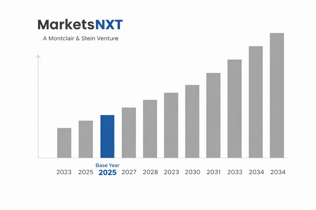
- ✓Base Year: 2025
- ✓Forecast Period: 2026–2034
- ✓Contrarian Insight: Taiwan's compound semiconductor advantage replicates its silicon success through the same mechanism — foundry model enabling fabless design companies globally to access world-class manufacturing without capital investment — but compound semiconductor foundry is 10 years behind silicon foundry in commercialisation maturity, giving Taiwanese compound foundries a first-mover positioning advantage that TSMC had in silicon in the 1990s
Market Overview
The Taiwanese compound semiconductor market was valued at approximately USD 3.18 billion in 2024 and is projected to reach approximately USD 12.4 billion by 2034, growing at a CAGR of 14.6%–18.1%. Taiwan is the world's largest compound semiconductor foundry market — WIN Semiconductors (GaAs RF), AWSC (GaN power), and Epistar (LED and optoelectronics) collectively serve 60%–70% of global fabless compound semiconductor design companies' outsourced manufacturing needs for RF front-ends, power amplifiers, and optoelectronic components. Taiwan's compound semiconductor industry has built its competitive position by extending the foundry model — pure-play outsourced manufacturing for design companies — from silicon into III-V materials, creating a globally unique compound semiconductor manufacturing ecosystem.
Taiwan's GaAs RF foundry sector — serving Qualcomm, Broadcom, Qorvo, and Skyworks' outsourced PA (power amplifier) and front-end module production — is the dominant revenue segment, representing approximately USD 1.8–2.0 billion of total Taiwanese compound semiconductor revenue in 2024. GaAs-based RF components in every 5G smartphone (PA, LNA, switch) and satellite communication system are predominantly manufactured at WIN Semiconductors (1.8 million 6-inch GaAs wafers/yr capacity) and smaller foundries. Taiwan's position in GaAs RF is structurally secure for the 5G era — but the 6G transition to terahertz frequencies (above 100 GHz) will require InP (indium phosphide) HEMT devices rather than GaAs, creating a technology transition risk that Taiwanese foundries are addressing through InP capability development.
Key Growth Drivers
5G smartphone and fixed wireless access (FWA) RF component demand is the current primary driver. Every 5G smartphone contains 3–6 GaAs power amplifier modules (for sub-6 GHz and millimetre-wave bands) and 1–2 GaN front-end components — representing USD 8–15 in compound semiconductor content per device at USD 600–1,000 smartphone ASP. Global 5G smartphone shipments of 700–800 million units annually in 2024–2025 create approximately USD 5.6–12 billion in compound RF component demand — with Taiwanese foundries manufacturing 60%–65% of the GaAs PA content. FWA router (home 5G broadband) adoption is adding incremental GaAs and GaN component demand as carriers deploy millimetre-wave FWA in US (Verizon, T-Mobile) and Asian markets.
GaN power device adoption in EV charging infrastructure and industrial power conversion is the fastest-growing compound semiconductor application. GaN-on-silicon transistors (Navitas Semiconductor, GaN Systems, Infineon GaN) are replacing silicon MOSFETs in EV onboard chargers (OBC), DC-DC converters, and fast chargers (45W–240W consumer chargers) — with GaN enabling 40%–60% size reduction and 95%+ efficiency versus silicon equivalents at equivalent power rating. Taiwan's AWSC (Advanced Wireless Semiconductor) is the primary outsourced GaN-on-silicon foundry for Navitas, GaN Systems, and other fabless GaN power designers — with AWSC expanding GaN power capacity from 15,000 to 40,000+ 8-inch wafers/month by 2026 to serve EV and charging market demand.
MicroLED display development is creating new compound semiconductor demand for GaN and AlGaInP epitaxy. MicroLED displays — used in Apple Vision Pro (Sony manufactured, Apple designed LED arrays), Samsung MicroLED wall displays, and automotive heads-up displays — require compound semiconductor LED arrays of 1–10 micron pixel pitch that conventional GaN LED manufacturing processes cannot economically achieve. Taiwan's Epistar and PlayNitride are the world's most advanced MicroLED epitaxy and transfer technology developers — with Apple's USD 1 billion MicroLED display investment (primarily at TSMC's packaging facility and Epistar's compound LED lines) making MicroLED a significant near-term compound semiconductor revenue stream in Taiwan.
Market Challenges
SiC substrate supply chain concentration creates technology access risk for Taiwan's SiC power foundry ambitions. SiC wafer production is dominated by Wolfspeed (US) and Coherent (II-VI, US) — controlling approximately 70%+ of global SiC substrate supply. US export control concerns about SiC substrate supply to Taiwan (given Taiwan's geopolitical sensitivity) and Wolfspeed's own SiC power device strategy (preferring to sell finished SiC MOSFETs rather than bare substrates to potential foundry competitors) create supply chain friction for Taiwanese SiC foundry development. Taiwan's GlobalWafers is developing domestic SiC substrate production — USD 500 million investment, targeting 50,000 substrates/month by 2026 — but currently remains dependent on US substrate supply for SiC device production.
Geopolitical cross-strait tension creates insurance and capital cost premium for Taiwanese compound semiconductor investment. Taiwan's geographical proximity to China (180 km at closest point) creates political risk premium of 200–400 basis points on semiconductor sector capital cost versus equivalent facilities in South Korea or Japan — an investor perception risk that is difficult to eliminate regardless of operational and technical fundamentals. Compound semiconductor capacity expansions by AWSC and WIN are proceeding despite geopolitical risk because fabless customers have no alternative outsourced manufacturing destination at equivalent quality — but the risk perception affects talent recruitment (engineers from US and European universities may prefer Japan or South Korea postings) and new investor entry into Taiwanese compound semiconductor capacity expansion financing.
Emerging Opportunities
The 3–5 year opportunity is optical interconnect compound semiconductor for AI data centre infrastructure. AI hyperscale data centres (NVIDIA H100/H200 GPU clusters) require optical interconnects between GPU servers — co-packaged optics (CPO) using InP or GaAs vertical cavity surface emitting lasers (VCSELs) and photodetectors at 800G, 1.6T, and 3.2T data rates. Taiwan's existing compound optoelectronic manufacturing base (Epistar VCSELs, Win Semi InGaP-HBT process for laser drivers) positions Taiwan as the primary manufacturing location for AI optical interconnect components. NVIDIA's co-packaged optics supply chain — targeting CPO in Blackwell successor GPU architectures — will drive USD 500 million–1 billion in new compound semiconductor demand in Taiwan by 2027–2028.
The 5–10 year opportunity is 6G sub-terahertz compound semiconductor for Samsung and Ericsson 6G base station supply. 6G base stations operating at 100–300 GHz sub-terahertz frequencies require InP HEMT (high electron mobility transistor) power amplifiers at frequencies where GaAs (current 5G PA technology) cannot operate at required efficiency. WIN Semiconductors is investing in InP HEMT process development targeting 100+ GHz operation — positioning Taiwan as the 6G RF front-end outsourced manufacturing hub analogous to its 5G GaAs dominance. First 6G commercial deployments in 2028–2030 (South Korea, Japan) will create InP foundry demand that Taiwan is uniquely positioned to serve from existing compound semiconductor manufacturing infrastructure.
Market at a Glance
| Parameter | Details |
|---|---|
| Market Size 2025 | Approximately USD 3.78 billion |
| Market Size 2034 | Approximately USD 12.4 billion |
| Market Growth Rate | 14.6%–18.1% |
| Largest Segment | GaAs RF Devices for 5G Smartphone and Base Station (WIN Semiconductors) |
| Fastest Growing Segment | GaN Power Devices for EV Charging and Industrial Conversion |
Leading Market Participants
- WIN Semiconductors (GaAs RF foundry)
- Advanced Wireless Semiconductor Company (AWSC)
- Epistar (compound LED and optoelectronics)
- GlobalWafers (compound semiconductor substrate)
- IQE Taiwan (compound semiconductor epitaxy)
Regulatory and Policy Environment
Taiwan's compound semiconductor industry operates under MOEA (Ministry of Economic Affairs) industrial policy — with compound semiconductor designated as a strategic advanced technology sector eligible for R&D tax credits of 25% (versus standard 15%) and accelerated depreciation for qualifying capital expenditure. NARL (National Applied Research Laboratories) and ITRI (Industrial Technology Research Institute) provide government-funded compound semiconductor process research that is transferred to industry through licensing arrangements — ITRI's compound semiconductor group has IP licensing relationships with WIN, AWSC, and Epistar covering epitaxy and device process technology.
Taiwan's export control framework for compound semiconductors is aligned with the Wassenaar Arrangement — requiring export licences for compound semiconductor manufacturing equipment (MOCVD reactors, MOVPE systems) exported to controlled destinations and for high-frequency InP and GaN devices above technical parameter thresholds. US BIS Entity List additions for Chinese semiconductor companies (Huawei, SMIC subsidiaries, compound semiconductor developers) affect Taiwanese compound semiconductor foundries' ability to serve Chinese fabless customers — WIN Semiconductors and AWSC have publicly stated compliance with US export control requirements, effectively restricting service to Chinese customers for technologies subject to US restrictions. This creates market access constraints in the Chinese compound semiconductor foundry market but positions Taiwan favourably as a trusted non-China manufacturing alternative for US and European fabless companies.
Long-Term Outlook
By 2034, Taiwan's compound semiconductor market will have diversified from GaAs RF dominance into GaN power (40%+ of revenue), InP photonics (optical AI interconnect), and MicroLED (Apple supply chain) — with total market scale tripling from 2024 driven by EV adoption and AI infrastructure demand. WIN Semiconductors' 8-inch GaN production expansion and AWSC's compound power device foundry capacity will position Taiwan as the world's largest GaN power foundry base — replicating the silicon foundry market share dominance that TSMC achieved in logic. TSMC's compound semiconductor integration (GaN in CoWoS packaging, silicon photonics integration) will create new hybrid compound-silicon product categories that leverage Taiwan's unique capability in both domains simultaneously.
The underweighted development in Taiwanese compound semiconductor analysis is the application of compound semiconductors in quantum computing hardware. Quantum computing requires qubits implemented in compound semiconductor materials — InAs quantum dots for topological qubits (Microsoft's approach), GaAs-based spin qubits (Delft University approach), and AlGaAs/GaAs heterostructure 2DEG qubits all require compound epitaxy at nanometre-precision layer control. Microsoft's topological qubit programme has established partnerships with InP and InAs MOCVD epitaxy providers — Taiwan's compound semiconductor epitaxy industry (Epistar, IQE Taiwan) has the material quality and process control required for quantum device epitaxy. If Microsoft's topological qubit commercialises, Taiwan's compound semiconductor sector could supply the qubit epitaxy for the global quantum computing industry — a potentially transformative long-term market position.
Frequently Asked Questions
Market Segmentation
- GaAs RF Devices (Power Amplifiers, LNA, Switches for 5G and WiFi)
- GaN Power Devices (EV Charger, Industrial Power Conversion)
- Compound Optoelectronics (VCSELs, LED Arrays, LiDAR Emitters)
- Others (InP High-Frequency Devices, AlN Substrates, SiC Power Devices)
- Smartphone and Mobile RF Front-End (5G PA, LNA, FEM)
- EV and EV Charging Infrastructure (GaN OBC, DC-DC)
- Data Centre Optical Interconnect (VCSEL, Photodetector)
- Consumer Electronics (WiFi 7, AR/VR Optics, MicroLED)
- Automotive Radar and LiDAR (GaN, GaAs components)
- Foundry Service to Fabless Design Companies (WIN, AWSC foundry model)
- IDM Direct Sales (Epistar, domestic LED and optoelectronic supply)
- TSMC Advanced Packaging Integration (CoWoS GaN power integration)
- Export via Contract Manufacturing to US, EU, Japan OEM Supply Chains
- Gallium Arsenide (GaAs) — RF and Optoelectronics
- Gallium Nitride (GaN) — Power and RF
- Indium Phosphide (InP) — High-Frequency and Photonics
- Silicon Carbide (SiC) — High-Power and High-Voltage
Table of Contents
Research Framework and Methodological Approach
Information
Procurement
Information
Analysis
Market Formulation
& Validation
Overview of Our Research Process
MarketsNXT follows a structured, multi-stage research framework designed to ensure accuracy, reliability, and strategic relevance of every published study. Our methodology integrates globally accepted research standards with industry best practices in data collection, modeling, verification, and insight generation.
1. Data Acquisition Strategy
Robust data collection is the foundation of our analytical process. MarketsNXT employs a layered sourcing model.
- Company annual reports & SEC filings
- Industry association publications
- Technical journals & white papers
- Government databases (World Bank, OECD)
- Paid commercial databases
- KOL Interviews (CEOs, Marketing Heads)
- Surveys with industry participants
- Distributor & supplier discussions
- End-user feedback loops
- Questionnaires for gap analysis
Analytical Modeling and Insight Development
After collection, datasets are processed and interpreted using multiple analytical techniques to identify baseline market values, demand patterns, growth drivers, constraints, and opportunity clusters.
2. Market Estimation Techniques
MarketsNXT applies multiple estimation pathways to strengthen forecast accuracy.
Bottom-up Approach
Aggregating granular demand data from country level to derive global figures.
Top-down Approach
Breaking down the parent industry market to identify the target serviceable market.
Supply Chain Anchored Forecasting
MarketsNXT integrates value chain intelligence into its forecasting structure to ensure commercial realism and operational alignment.
Supply-Side Evaluation
Revenue and capacity estimates are developed through company financial reviews, product portfolio mapping, benchmarking of competitive positioning, and commercialization tracking.
3. Market Engineering & Validation
Market engineering involves the triangulation of data from multiple sources to minimize errors.
Extensive gathering of raw data.
Statistical regression & trend analysis.
Cross-verification with experts.
Publication of market study.
Client-Centric Research Delivery
MarketsNXT positions research delivery as a collaborative engagement rather than a static information transfer. Analysts work with clients to clarify objectives, interpret findings, and connect insights to strategic decisions.