UK Extreme Ultraviolet (EUV) Lithography Market Size, Share & Forecast 2026–2034
Report Highlights
- ✓Country: United Kingdom
- ✓Market: Extreme Ultraviolet (EUV) Lithography
- ✓Market Size 2024: USD 312.4 Million
- ✓Market Size 2032: USD 891.7 Million
- ✓CAGR: 13.9%
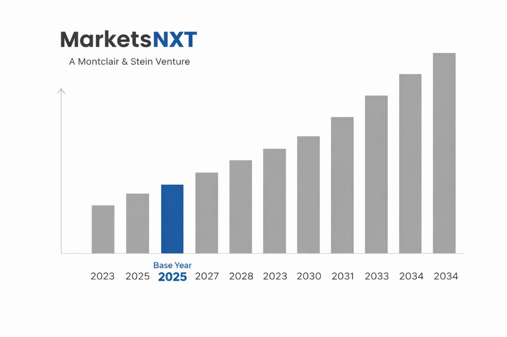
- ✓Base Year: 2025
- ✓Forecast Period: 2026–2032
Analyst Recommendation — Acquire Before Tariff Escalation: Foreign investors evaluating UK EUV-adjacent positions should acquire stakes in UK nanofabrication service providers before Q3 2026, when post-Brexit semiconductor trade negotiations with the EU are expected to alter equipment import tariff structures and increase entry costs materially.
UK Extreme Ultraviolet Lithography: Market Overview
The UK EUV lithography market occupies a structurally distinct position within the global semiconductor landscape. Unlike South Korea, Taiwan, or the United States — where EUV is deployed primarily at high-volume logic and memory fabs — the UK market is concentrated around research institutions, government-backed pilot lines, and low-to-mid volume specialty semiconductor manufacturing. The UK's installed base of EUV-capable or EUV-adjacent nanofabrication tools remains limited compared to Asia-Pacific peers, but demand from defence electronics, quantum computing research, and compound semiconductor applications is creating a differentiated, high-value demand profile that diverges sharply from global volume-driven norms.
The UK's semiconductor sector generates approximately £9.9 billion in annual revenue, yet domestic EUV tool ownership and deployment capacity trail significantly behind the sector's broader ambitions. Newport Wafer Fab in Wales, acquired by Nexperia and subsequently subject to a government divestment order under the National Security and Investment Act 2021, remains the most high-profile UK fab with relevance to advanced lithography investment. The market's 2024 valuation of USD 312.4 million reflects equipment procurement, ancillary services, photomask supply chains, and research infrastructure combined — a composite structure that makes the UK EUV market more services- and IP-weighted than its global counterparts.
Growth Drivers in the UK EUV Lithography Market
The UK Government's National Semiconductor Strategy, published in May 2023 with an initial commitment of £1 billion over ten years, is the primary structural driver accelerating EUV lithography investment. This strategy explicitly funds advanced fabrication research, compound semiconductor scale-up, and design capability — all of which require access to EUV-level patterning or EUV simulation environments. The UKRI-administered £38 million semiconductor grants disbursed in 2023–2024 directly supported nanofabrication infrastructure at universities and research institutes, creating institutional demand pipelines that feed into equipment procurement cycles with three-to-five year horizons.
The UK's leadership in compound semiconductors — centred on the CSconnected cluster in Wales and IQE plc's manufacturing network — is a second driver pushing lithography capability requirements toward EUV-compatible nodes. IQE's compound wafer production for 5G, photonics, and power electronics increasingly demands sub-10nm patterning precision that EUV uniquely enables. Additionally, the UK Ministry of Defence's investment in sovereign semiconductor capability under the Defence and Security Industrial Strategy is generating classified demand for advanced lithography tools applicable to radar, electronic warfare, and satellite communication component manufacturing, adding a non-commercial demand layer that reinforces overall market growth through the forecast period.
Market Restraints and Entry Barriers
The most significant entry barrier in the UK EUV lithography market is the extreme capital intensity of EUV tool acquisition combined with ASML's monopoly supply position. A single ASML NXE:3800E system costs approximately USD 380 million, and ASML's allocation queue prioritises TSMC, Samsung, and Intel — meaning UK buyers face multi-year lead times regardless of funding availability. The UK lacks the domestic semiconductor equipment manufacturing base required to build alternative EUV light sources or optics, making ASML dependency structural rather than transitional. This single-supplier chokepoint creates a ceiling on the pace of UK EUV deployment that no domestic policy intervention can currently resolve.
Regulatory complexity under the National Security and Investment Act 2021 introduces a second layer of friction for foreign investors seeking to enter the UK EUV supply chain. The Act mandates mandatory notification for acquisitions in the semiconductor sector, with BEIS (now the Department for Science, Innovation and Technology) empowered to block or impose conditions on transactions. This oversight regime, while intended to protect sovereign capability, has demonstrably slowed inbound investment decisions — the Nexperia-Newport Wafer Fab case required 18 months of review before the divestment order was issued in 2023. Combined with post-Brexit trade frictions affecting optical components and high-purity chemical imports from EU suppliers, these barriers materially extend market entry timelines for new participants.
Market Opportunities in the UK EUV Lithography Market
The most immediate and addressable opportunity lies in EUV ancillary services: photomask inspection, pellicle supply, resist chemistry, and metrology equipment. The UK has no domestic EUV pellicle manufacturer, and the global supply is dominated by ASML's own pellicle unit and Mitsui Chemicals. A UK-based or UK-entering manufacturer capable of qualifying EUV pellicles for research-grade applications — where contamination tolerances differ from production environments — faces an addressable market estimated at USD 45–60 million by 2028 within the UK and adjacent European research ecosystem alone. This niche is currently unserved domestically and structurally protected from Asian competition by proximity and lead-time advantages.
A second opportunity exists in EUV-compatible photoresist development, where the UK's strong chemistry and materials science base creates genuine competitive advantage. Companies such as Merck KGaA's UK operations and spin-outs from the University of Edinburgh's chemistry departments are positioned to commercialise metal-oxide EUV resists that outperform conventional chemically amplified resists at sub-7nm nodes. The Henry Royce Institute's shared infrastructure programme provides subsidised access to advanced characterisation equipment that reduces the R&D cost barrier for new resist entrants. Investors targeting the UK EUV market via materials rather than capital equipment acquisition face a lower capital threshold, faster time-to-revenue, and a defensible IP position anchored in UK academic outputs.
Market at a Glance
| Metric | Detail |
|---|---|
| Market Size 2024 | USD 312.4 Million |
| Market Size 2032 | USD 891.7 Million |
| Growth Rate | 13.9% CAGR |
| Most Critical Decision Factor | ASML equipment allocation queue and lead times |
| Largest Region | South East England and Wales Compound Semiconductor Cluster |
| Competitive Structure | Monopoly equipment supply, fragmented services |
Leading Market Participants
- ASML UK Ltd
- IQE plc
- Merck KGaA (UK Operations)
- Compound Semiconductor Centre (CSC)
- Newport Wafer Fab (Nexperia)
- Sifted Semiconductor (UKRI-backed)
- Coherent Corp (UK Photonics Division)
- Oxford Instruments
- SPTS Technologies (Orbotech Group)
- Renishaw plc
Regulatory and Policy Environment
The National Security and Investment Act 2021 is the governing legislation for semiconductor sector transactions in the UK, requiring mandatory notification to the Investment Security Unit within the Department for Science, Innovation and Technology (DSIT) for any acquisition of 25% or more in a qualifying semiconductor entity. The UK Semiconductor Strategy (2023) established the Semiconductor Advisory Panel and allocated funding through Innovate UK for advanced fabrication research, including a £200 million commitment to compound semiconductor scale-up specifically referencing advanced lithography requirements. The CHIPS-equivalent UK framework remains less financially endowed than the US CHIPS and Science Act or the EU Chips Act, but DSIT's 2024 consultation on sovereign fab investment incentives signals forthcoming capital grant mechanisms analogous to EU Important Projects of Common European Interest structures.
Environmental compliance under the UK Environment Act 2021 imposes specific obligations on EUV facility operators regarding per- and polyfluoroalkyl substance (PFAS) handling — materials widely used in EUV photoresist chemistries — with new reporting requirements effective from January 2025. The Health and Safety Executive regulates high-power laser and plasma-discharge systems used in EUV light source modules under the Control of Electromagnetic Fields at Work Regulations 2016, requiring documented risk assessments and operator certification for all EUV-adjacent equipment. Import licensing for dual-use optical components — governed by the UK Strategic Export Control List following Brexit — adds procurement complexity for EUV optics sourced from non-UK suppliers, with ECJU licence processing times averaging eight to twelve weeks for controlled photonics components.
Long-Term Outlook for the UK EUV Lithography Market
By 2032, the UK EUV lithography market is projected to reach USD 891.7 million, driven by the maturation of the National Semiconductor Strategy's capital deployment pipeline, the scaling of compound semiconductor fabs in Wales and the Midlands, and expanding defence electronics procurement. The market will bifurcate into a research-grade segment — served by shared-access facilities at the Henry Royce Institute, the National Physical Laboratory, and university nanofabrication centres — and a nascent commercial production segment anchored by one or two ASML tool acquisitions at government-supported pilot fabs. The research segment will account for approximately 55% of total market value by 2032 due to the capital intensity and institutional ownership structure of UK EUV infrastructure.
The long-term competitive position of UK participants in the global EUV value chain depends critically on whether DSIT's forthcoming fab investment incentive scheme reaches parity with EU Chips Act state aid levels, currently set at up to 40% capital grants for first-of-kind facilities. Without competitive grant parity, UK fab operators will continue to lose ASML allocation priority to EU counterparts. However, the UK's comparative advantage in EUV-adjacent photonics, resist chemistry, and metrology instrumentation — sectors where Oxford Instruments and Renishaw already hold global technology leadership — creates a viable export-oriented market trajectory that sustains 13.9% CAGR even absent large-scale domestic wafer production growth through the forecast period.
Market Segmentation
By Component
- EUV Light Sources
- Optical Systems and Mirrors
- Photomasks and Pellicles
- EUV Photoresists
- Metrology and Inspection Equipment
- Wafer Stages and Handlers
By Application
- Logic Semiconductor Manufacturing
- Compound Semiconductor Fabrication
- Defence and Aerospace Electronics
- Photonics and Quantum Device Research
- Academic and Research Institutions
By End User
- Integrated Device Manufacturers
- Pure-Play Foundries
- University Nanofabrication Centres
- Government Research Institutes
- Defence Contractors
By Technology Node
- Sub-5nm
- 5nm to 7nm
- 7nm to 10nm
- Above 10nm EUV-Compatible
Frequently Asked Questions
Entry via EUV ancillary services — resist chemistry, metrology, or photomask inspection — requires USD 5–15 million in initial R&D and qualification capital, substantially below the USD 380 million cost of a single ASML EUV tool. UKRI grant co-funding covers up to 70% of eligible R&D costs for qualifying UK-registered entities under the Innovate UK Launchpad programme.
Yes — the Act mandates mandatory notification for acquisitions reaching 25%, 50%, or 75% voting rights thresholds in any entity active in the semiconductor sector, including EUV supply chain businesses. Voluntary notification is also available and strongly advisable for acquisitions below 25% where national security considerations are present.
South Wales hosts the CSconnected compound semiconductor cluster and Newport Wafer Fab, providing the densest concentration of EUV-adjacent manufacturing and supply chain activity in the UK. The Oxford-Cambridge Arc and Manchester (home to the Henry Royce Institute) are the leading research-oriented entry points for materials and instrumentation businesses.
EUV-grade optical components classified under UK Global Tariff headings 9001 and 9013 face 0–3.7% import duties, but dual-use items on the UK Strategic Export Control List require Export Control Joint Unit licences that add eight to twelve weeks to procurement timelines. Suppliers should pre-qualify components against the UK Military List and UK Dual-Use List before contracting.
The most viable exit pathways are strategic acquisition by global semiconductor equipment majors — ASML, Tokyo Electron, or Applied Materials — which have each made UK acquisitions in adjacent photonics and metrology sectors within the past five years. Secondary exits via AIM-listed semiconductor holding vehicles or direct sale to government-backed sovereign capability funds represent additional options as DSIT's investment incentive framework matures post-2026.
Frequently Asked Questions
Market Segmentation
- EUV Light Sources
- Optical Systems and Mirrors
- Photomasks and Pellicles
- EUV Photoresists
- Metrology and Inspection Equipment
- Wafer Stages and Handlers
- Logic Semiconductor Manufacturing
- Compound Semiconductor Fabrication
- Defence and Aerospace Electronics
- Photonics and Quantum Device Research
- Academic and Research Institutions
- Integrated Device Manufacturers
- Pure-Play Foundries
- University Nanofabrication Centres
- Government Research Institutes
- Defence Contractors
- Sub-5nm
- 5nm to 7nm
- 7nm to 10nm
- Above 10nm EUV-Compatible
Table of Contents
Research Framework and Methodological Approach
Information
Procurement
Information
Analysis
Market Formulation
& Validation
Overview of Our Research Process
MarketsNXT follows a structured, multi-stage research framework designed to ensure accuracy, reliability, and strategic relevance of every published study. Our methodology integrates globally accepted research standards with industry best practices in data collection, modeling, verification, and insight generation.
1. Data Acquisition Strategy
Robust data collection is the foundation of our analytical process. MarketsNXT employs a layered sourcing model.
- Company annual reports & SEC filings
- Industry association publications
- Technical journals & white papers
- Government databases (World Bank, OECD)
- Paid commercial databases
- KOL Interviews (CEOs, Marketing Heads)
- Surveys with industry participants
- Distributor & supplier discussions
- End-user feedback loops
- Questionnaires for gap analysis
Analytical Modeling and Insight Development
After collection, datasets are processed and interpreted using multiple analytical techniques to identify baseline market values, demand patterns, growth drivers, constraints, and opportunity clusters.
2. Market Estimation Techniques
MarketsNXT applies multiple estimation pathways to strengthen forecast accuracy.
Bottom-up Approach
Aggregating granular demand data from country level to derive global figures.
Top-down Approach
Breaking down the parent industry market to identify the target serviceable market.
Supply Chain Anchored Forecasting
MarketsNXT integrates value chain intelligence into its forecasting structure to ensure commercial realism and operational alignment.
Supply-Side Evaluation
Revenue and capacity estimates are developed through company financial reviews, product portfolio mapping, benchmarking of competitive positioning, and commercialization tracking.
3. Market Engineering & Validation
Market engineering involves the triangulation of data from multiple sources to minimize errors.
Extensive gathering of raw data.
Statistical regression & trend analysis.
Cross-verification with experts.
Publication of market study.
Client-Centric Research Delivery
MarketsNXT positions research delivery as a collaborative engagement rather than a static information transfer. Analysts work with clients to clarify objectives, interpret findings, and connect insights to strategic decisions.