
U.S. 4 Inches Semi-Insulating Silicon Carbide Wafer Market Size, Share & Forecast 2026–2032
Report Highlights
- ✓Country: United States
- ✓Market: 4 Inches Semi-Insulating Silicon Carbide Wafer
- ✓Market Size 2024: USD 187.4 Million
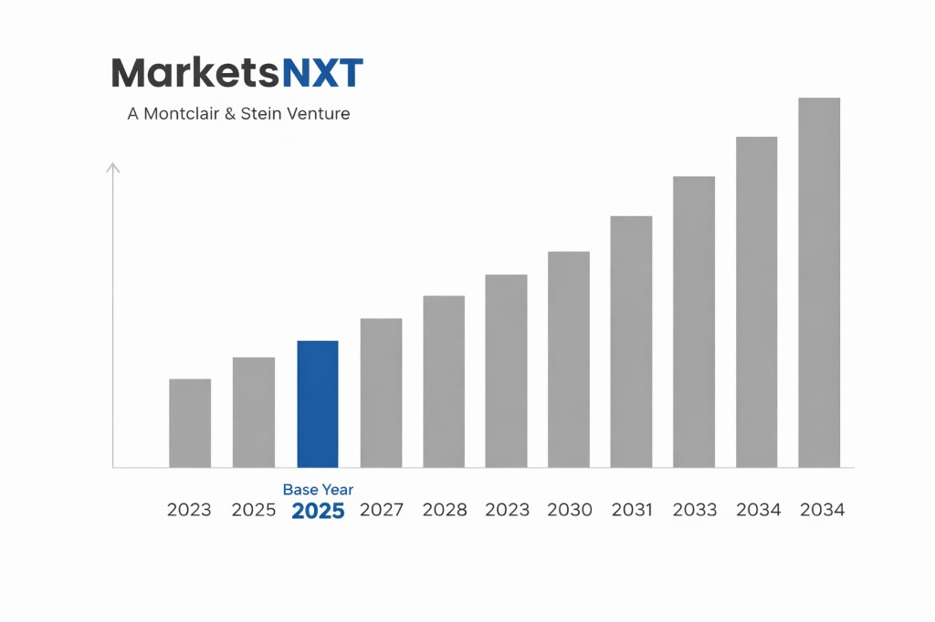
- ✓Market Size 2032: USD 541.8 Million
- ✓CAGR: 14.2%
- ✓Base Year: 2025
- ✓Forecast Period: 2026–2032
Analyst Recommendation — Enter Via Defense Channel: Foreign and domestic entrants targeting this market should secure a ITAR-registered U.S. distribution partner and pursue qualification under MIL-PRF-32535 by Q3 2026, before the next DoD multi-year SiC substrate procurement cycle closes in early 2027.
U.S. 4-Inch Semi-Insulating Silicon Carbide Wafer Market: Market Overview
The U.S. market for 4-inch semi-insulating silicon carbide wafers occupies a specialized but strategically critical segment within the broader SiC substrate industry. Unlike conductive SiC wafers used in power electronics, semi-insulating grades are required for radio frequency devices, high-electron-mobility transistors, and military-grade radar systems, commanding a significant price premium per wafer. The U.S. market generated USD 187.4 million in 2024 and is characterized by a heavily consolidated domestic supply base, with procurement tightly linked to defense contractor qualification requirements and commercial 5G infrastructure buildout.
What distinguishes this market from global norms is the dominant influence of U.S. government procurement and export control frameworks. The International Traffic in Arms Regulations and Export Administration Regulations impose strict controls on semi-insulating SiC wafer exports to certain jurisdictions, effectively insulating the domestic market from certain low-cost Asian suppliers. This regulatory moat supports premium domestic pricing and limits the competitive disruption typically seen in commoditizing semiconductor substrate markets. The market structure is therefore less price-elastic than international equivalents, with qualification cycles and national security requirements acting as persistent structural barriers.
Growth Drivers in the U.S. 4-Inch Semi-Insulating SiC Wafer Market
Three demand drivers are accelerating U.S. market growth through 2032. First, the Department of Defense's Microelectronics Commons program, funded at USD 2 billion under the CHIPS and Science Act, is directly channeling capital into domestic SiC substrate development hubs. This initiative specifically targets wide-bandgap semiconductor materials including semi-insulating SiC for next-generation radar, electronic warfare, and satellite communication platforms. Raytheon Technologies and Northrop Grumman have both publicly cited SiC substrate supply security as a program-critical procurement priority for phased-array radar systems entering production through 2027.
Second, the commercial 5G and emerging 6G infrastructure rollout is generating sustained demand for GaN-on-SiC power amplifiers that require semi-insulating 4-inch substrates. Ericsson and Nokia's U.S. manufacturing partnerships are qualifying SiC-based RF front-end components at scale, sustaining demand independent of the defense channel. Third, the CHIPS Act Section 9902 incentive program, offering a 25% advanced manufacturing investment tax credit, is stimulating capacity investment among U.S.-based substrate producers, creating a pull-through effect on raw wafer demand as new device fabrication lines reach qualification milestones between 2025 and 2028.
Market Restraints and Entry Barriers
The most significant entry barrier is the lengthy and capital-intensive customer qualification process specific to this market. Defense OEMs require suppliers to complete MIL-PRF-32535 qualification and Defense Logistics Agency Land and Maritime registration, a process that routinely takes 18 to 36 months and costs new entrants between USD 3 million and USD 8 million in testing and documentation. Wolfspeed's established qualification status across Lockheed Martin, Raytheon, and L3Harris supply chains creates a structural incumbency advantage that new domestic or foreign suppliers cannot overcome quickly regardless of wafer quality or pricing competitiveness.
A second major restraint is the ITAR registration requirement for any entity handling semi-insulating SiC wafers destined for defense applications. Foreign-owned companies must navigate the Directorate of Defense Trade Controls licensing process, which adds compliance overhead, limits foreign direct investment structures in U.S. SiC facilities, and creates uncertainty around technology transfer agreements. Additionally, the episodic nature of DoD multi-year procurement contracts means that demand arrives in concentrated tranches rather than steady volumes, complicating production planning for smaller suppliers and reinforcing reliance on Wolfspeed as the primary credentialed domestic source. Raw material constraints around high-purity silicon carbide powder further tighten supply chain resilience.
Market Opportunities in the U.S. 4-Inch Semi-Insulating SiC Wafer Market
The most addressable near-term opportunity lies in serving second-tier defense subcontractors and commercial RF device manufacturers who cannot access Wolfspeed's wafer allocation due to capacity constraints. Wolfspeed's announced capacity expansion at Siler City is not expected to reach full production scale until late 2026, creating an estimated 18-month supply gap for qualified 4-inch semi-insulating substrates. Suppliers with existing ITAR registration and preliminary qualification data, particularly those based in allied nations such as Japan or Germany, represent the most credible candidates to fill this gap through U.S.-registered distribution arrangements.
A second opportunity exists in the photonics and quantum computing substrate segment, where semi-insulating SiC's high resistivity and thermal conductivity are driving early-stage adoption for qubit packaging and integrated photonic platforms. DARPA's Quantum Benchmarking Initiative and the National Quantum Initiative Act programs are funding substrate material evaluations in which semi-insulating 4-inch SiC wafers are included as primary candidates. The addressable market within quantum and photonics remains modest at approximately USD 12 to USD 18 million annually through 2028 but carries significantly higher average selling prices, making it attractive for specialty suppliers willing to invest in application-specific wafer surface preparation capabilities ahead of demand maturation.
Market at a Glance
| Metric | Detail |
|---|---|
| Market Size 2024 | USD 187.4 Million |
| Market Size 2032 | USD 541.8 Million |
| Growth Rate (CAGR) | 14.2% |
| Most Critical Decision Factor | Defense qualification status and ITAR compliance |
| Largest Region | Southeast U.S. (North Carolina, Research Triangle) |
| Competitive Structure | Highly consolidated, single domestic dominant supplier |
Leading Market Participants
- Wolfspeed, Inc.
- II-VI Incorporated (Coherent Corp.)
- CREE Research
- Dow Chemical Company (Advanced Silicon Carbide)
- Norstel AB (U.S. operations)
- SiCrystal GmbH (U.S. distribution via ROHM)
- TankeBlue Semiconductor (U.S.-registered entity)
- PAM-XIAMEN (U.S. channel)
- DuPont Electronics
- MTI Corporation
Regulatory and Policy Environment
The regulatory framework governing 4-inch semi-insulating SiC wafers in the United States is anchored by three primary instruments. The Export Administration Regulations under the Bureau of Industry and Security classify semi-insulating SiC substrates under ECCN 3C005, requiring export licenses for shipments to countries subject to technology controls including China and Russia. Separately, ITAR administered by the Directorate of Defense Trade Controls applies when wafers are destined for defense articles under the U.S. Munitions List Category XI. The CHIPS and Science Act of 2022 Section 9902 provides a 25% investment tax credit for qualifying advanced semiconductor manufacturing equipment purchases, directly incentivizing domestic substrate capacity expansion through a credit structure available through fiscal year 2026.
The Department of Commerce's National Institute of Standards and Technology administers the Metrology and Standards Program for wide-bandgap semiconductors, which sets reference wafer specifications adopted by JEDEC Standard JESD235 for SiC substrate characterization. Compliance with these specifications is required for wafers entering DoD supply chains through DLA Land and Maritime qualification under QPL-32535. The Federal Acquisition Regulation Part 25 domestic content requirements and the Berry Amendment restrict non-U.S.-origin substrates in certain defense procurements, reinforcing domestic supplier advantages. New entrants should monitor the anticipated 2026 revision to EAR Part 742 which is expected to tighten multilateral controls on SiC substrate exports under the Wassenaar Arrangement's emerging technology annex updates.
Long-Term Outlook for the U.S. 4-Inch Semi-Insulating SiC Wafer Market
By 2032, the U.S. 4-inch semi-insulating SiC wafer market is projected to reach USD 541.8 million, driven by the maturation of next-generation defense radar programs and continued GaN-on-SiC device proliferation in commercial wireless infrastructure. The market will not be displaced by 6-inch wafer migration in this segment within the forecast window; defense platform qualification cycles lock in 4-inch specifications for programs with 10 to 15-year production horizons, including the F-35 Electronic Warfare Modernization Program and the Next Generation Interceptor. Wolfspeed's expanded North Carolina capacity will serve as the primary domestic supply anchor, though qualification of at least one additional domestic supplier is a stated objective within DoD's industrial base resilience strategy.
The long-term structural tension in this market is between domestic supply security imperatives and cost competitiveness. As commercial 5G demand eventually plateaus and defense procurement consolidates around qualified vendors, margin pressure will intensify for peripheral suppliers. Entrants who establish qualification and volume relationships before the 2027 DoD multi-year procurement cycle will secure positions that are extremely difficult to displace. The quantum computing and photonics segments will emerge as a meaningful secondary revenue stream by 2030, potentially contributing USD 30 to USD 40 million annually as substrate surface quality requirements mature into standardized procurement specifications aligned with the National Quantum Initiative's Phase III milestones.
Frequently Asked Questions
Market Segmentation
- Device Grade
- Research Grade
- Epi-Ready Grade
- Dummy Grade
- RF and Microwave Devices
- Defense and Radar Systems
- 5G Infrastructure
- Photonics
- Quantum Computing
- Power Amplifiers
- High Resistivity (greater than 10,000 ohm-cm)
- Ultra-High Resistivity (greater than 100,000 ohm-cm)
- Standard Semi-Insulating
- Direct OEM Supply
- Defense Qualified Distribution
- Research Institution Procurement
- Spot Market and Broker
Table of Contents
Research Framework and Methodological Approach
Information
Procurement
Information
Analysis
Market Formulation
& Validation
Overview of Our Research Process
MarketsNXT follows a structured, multi-stage research framework designed to ensure accuracy, reliability, and strategic relevance of every published study. Our methodology integrates globally accepted research standards with industry best practices in data collection, modeling, verification, and insight generation.
1. Data Acquisition Strategy
Robust data collection is the foundation of our analytical process. MarketsNXT employs a layered sourcing model.
- Company annual reports & SEC filings
- Industry association publications
- Technical journals & white papers
- Government databases (World Bank, OECD)
- Paid commercial databases
- KOL Interviews (CEOs, Marketing Heads)
- Surveys with industry participants
- Distributor & supplier discussions
- End-user feedback loops
- Questionnaires for gap analysis
Analytical Modeling and Insight Development
After collection, datasets are processed and interpreted using multiple analytical techniques to identify baseline market values, demand patterns, growth drivers, constraints, and opportunity clusters.
2. Market Estimation Techniques
MarketsNXT applies multiple estimation pathways to strengthen forecast accuracy.
Bottom-up Approach
Aggregating granular demand data from country level to derive global figures.
Top-down Approach
Breaking down the parent industry market to identify the target serviceable market.
Supply Chain Anchored Forecasting
MarketsNXT integrates value chain intelligence into its forecasting structure to ensure commercial realism and operational alignment.
Supply-Side Evaluation
Revenue and capacity estimates are developed through company financial reviews, product portfolio mapping, benchmarking of competitive positioning, and commercialization tracking.
3. Market Engineering & Validation
Market engineering involves the triangulation of data from multiple sources to minimize errors.
Extensive gathering of raw data.
Statistical regression & trend analysis.
Cross-verification with experts.
Publication of market study.
Client-Centric Research Delivery
MarketsNXT positions research delivery as a collaborative engagement rather than a static information transfer. Analysts work with clients to clarify objectives, interpret findings, and connect insights to strategic decisions.