U.S. Nanofilms Market Size, Share & Forecast 2026–2032
Report Highlights
- ✓Country: United States
- ✓Market: U.S. Nanofilms Market
- ✓Market Size 2024: USD 6.8 billion
- ✓Market Size 2032: USD 12.9 billion
- ✓CAGR: 8.3%
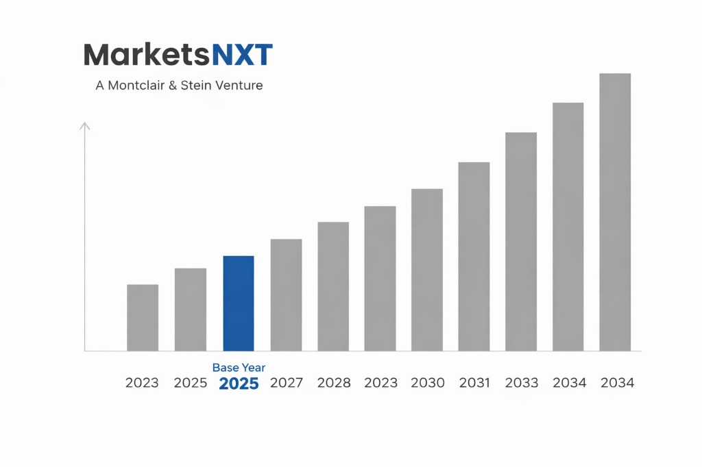
- ✓Base Year: 2025
- ✓Forecast Period: 2026-2032
Analyst Recommendation — Secure Midwest Capacity Now: Investors and buyers should secure Arizona or Ohio coating capacity before the 2026 fab ramp tightens qualification slots. Target CHIPS Act-linked co-location deals by Q3 2026, since early qualification determines second-source eligibility.
Nanofilms in the U.S.: Market Overview
The U.S. nanofilms market was valued at USD 6.8 billion in 2024 and accounts for roughly 26% of global nanofilm revenue, making it the largest single national market outside Asia-Pacific. Unlike the global market, which is driven by consumer electronics assembly in Taiwan, South Korea and China, U.S. demand is concentrated in semiconductor fabrication, aerospace coatings and architectural glass. Domestic players sell into long qualification cycles, often 12 to 24 months, which rewards incumbents.
Structurally, the market splits into two tiers. Tier one is fab-grade thin films sold by Applied Materials and Lam Research as part of capital equipment programs, while tier two is industrial and optical coatings sold through specialist suppliers such as Kurt J. Lesker Company and regional job shops in Pennsylvania, Minnesota and Ohio. Tier one carries higher margins but a narrower buyer base, which shapes how new entrants should price their offers.
Growth Drivers for Nanofilms in the United States
The CHIPS and Science Act of 2022 allocates USD 52.7 billion to semiconductor research and manufacturing, including USD 39 billion in manufacturing incentives administered by the Department of Commerce. Intel's New Albany, Ohio campus and TSMC's Phoenix, Arizona fabs require atomic layer deposition films for gate dielectrics and interconnects, creating sustained demand for nanofilm process materials through the forecast period. Each leading-edge fab consumes thin-film materials across hundreds of process steps.
The Inflation Reduction Act of 2022 supports domestic thin-film solar through the Section 45X advanced manufacturing production credit, which First Solar uses to justify its manufacturing footprint in Ohio. Encapsulation barrier films and anti-reflective coatings for these modules are specified in U.S. supply contracts. Separately, defense programs administered by the Department of Defense require nanocoated optics and corrosion-resistant films for aerospace platforms, sustaining a premium niche.
Market Restraints and Entry Barriers
Chemical approvals form the first barrier. Any nanofilm precursor that is a new chemical substance must clear EPA review under Section 5 of the Toxic Substances Control Act, as amended by the Frank R. Lautenberg Chemical Safety for the 21st Century Act of 2016. The Section 5 review period runs 90 days and can extend by another 90 days, so a novel precursor can delay commercial launch by half a year before the first wafer is coated.
Qualification and state-level restrictions compound the problem. Semiconductor and aerospace buyers typically require 12 to 24 months of customer qualification, favoring incumbents such as Applied Materials. Minnesota's PFAS restrictions under Amara's Law phase in product bans from 2025 onward, which narrows fluorinated film chemistries. Entrants also face Buy American requirements under DFARS for defense programs.
Market Opportunities in the United States
Advanced packaging is the nearest entry point. Amkor Technology's Peoria, Arizona campus will run wafer-level packaging that requires barrier and dielectric nanofilms, and we estimate a USD 1.1 billion addressable pool for U.S.-sourced film materials and coating services by 2032. Suppliers that qualify before the campus reaches volume production will secure multi-year supply agreements with local process engineers.
Defense and medical coatings offer a second route. Department of Defense programs under DFARS domestic sourcing rules favor U.S.-made corrosion-resistant and optical nanofilms, and we estimate an addressable USD 0.9 billion across aerospace and defense by 2032. In medtech, FDA 510(k) clearance for antimicrobial nanocoatings on hospital surfaces provides a clear regulatory path for specialist coaters in Massachusetts and Minnesota.
Market at a Glance
| Metric | Value |
|---|---|
| Market Size 2024 | USD 6.8 billion |
| Market Size 2032 | USD 12.9 billion |
| Growth Rate (CAGR) | 8.3% |
| Most Critical Decision Factor | Customer qualification timeline and CHIPS-linked site selection |
| Largest Region | Midwest, led by Ohio and Minnesota |
| Competitive Structure | Concentrated top tier, fragmented specialist coaters |
Leading Market Participants
- Applied Materials
- Lam Research
- Corning
- 3M
- Honeywell
- Entegris
- Dow
- PPG Industries
- Cima NanoTech
- Kurt J. Lesker Company
Regulatory and Policy Environment
Chemical oversight sits with the EPA under the Toxic Substances Control Act as amended by the Lautenberg Act of 2016, while OSHA and NIOSH set workplace exposure guidance for engineered nanomaterials. The National Nanotechnology Initiative, coordinated through the National Science and Technology Council, funds research and standards work at NIST, with annual federal nanotechnology R&D funding exceeding USD 1.7 billion.
Industrial policy is the main subsidy channel. The CHIPS and Science Act provides USD 39 billion in manufacturing incentives, while Section 48D of the Internal Revenue Code grants a 25% investment tax credit on qualified semiconductor manufacturing investment for projects beginning construction before January 1, 2027. Minnesota's Amara's Law requires PFAS reporting and phased product restrictions, so film chemistries must be documented before shipment.
Long-Term Outlook for Nanofilms in the U.S.
By 2032 the U.S. nanofilms market should reach USD 12.9 billion, with semiconductor and advanced packaging comprising the largest share and the Midwest overtaking California as the leading production base. Demand growth will concentrate in fab-adjacent supply, which favors companies with domestic production capacity over importers.
Competitive dynamics will shift toward consolidation among mid-sized coaters, as CHIPS-funded fabs demand traceable supply chains and tier-one equipment makers such as Applied Materials and Lam Research bundle film materials into tool contracts. Entrants that secure qualification by 2028 will be positioned for the 2030 capacity cycle.
Frequently Asked Questions
Market Segmentation
- Semiconductor and Electronics
- Architectural and Low-E Glass
- Aerospace and Defense Coatings
- Medical Devices
- Energy and Solar Modules
- Atomic Layer Deposition
- Physical Vapor Deposition
- Chemical Vapor Deposition
- Sol-Gel Coating
- Sputtering
Table of Contents
Research Framework and Methodological Approach
Information
Procurement
Information
Analysis
Market Formulation
& Validation
Overview of Our Research Process
MarketsNXT follows a structured, multi-stage research framework designed to ensure accuracy, reliability, and strategic relevance of every published study. Our methodology integrates globally accepted research standards with industry best practices in data collection, modeling, verification, and insight generation.
1. Data Acquisition Strategy
Robust data collection is the foundation of our analytical process. MarketsNXT employs a layered sourcing model.
- Company annual reports & SEC filings
- Industry association publications
- Technical journals & white papers
- Government databases (World Bank, OECD)
- Paid commercial databases
- KOL Interviews (CEOs, Marketing Heads)
- Surveys with industry participants
- Distributor & supplier discussions
- End-user feedback loops
- Questionnaires for gap analysis
Analytical Modeling and Insight Development
After collection, datasets are processed and interpreted using multiple analytical techniques to identify baseline market values, demand patterns, growth drivers, constraints, and opportunity clusters.
2. Market Estimation Techniques
MarketsNXT applies multiple estimation pathways to strengthen forecast accuracy.
Bottom-up Approach
Aggregating granular demand data from country level to derive global figures.
Top-down Approach
Breaking down the parent industry market to identify the target serviceable market.
Supply Chain Anchored Forecasting
MarketsNXT integrates value chain intelligence into its forecasting structure to ensure commercial realism and operational alignment.
Supply-Side Evaluation
Revenue and capacity estimates are developed through company financial reviews, product portfolio mapping, benchmarking of competitive positioning, and commercialization tracking.
3. Market Engineering & Validation
Market engineering involves the triangulation of data from multiple sources to minimize errors.
Extensive gathering of raw data.
Statistical regression & trend analysis.
Cross-verification with experts.
Publication of market study.
Client-Centric Research Delivery
MarketsNXT positions research delivery as a collaborative engagement rather than a static information transfer. Analysts work with clients to clarify objectives, interpret findings, and connect insights to strategic decisions.