U.S. Semiconductor Fabrication Materials Market Size, Share & Forecast 2026–2032
Report Highlights
- ✓Country: United States
- ✓Market: U.S. Semiconductor Fabrication Materials Market
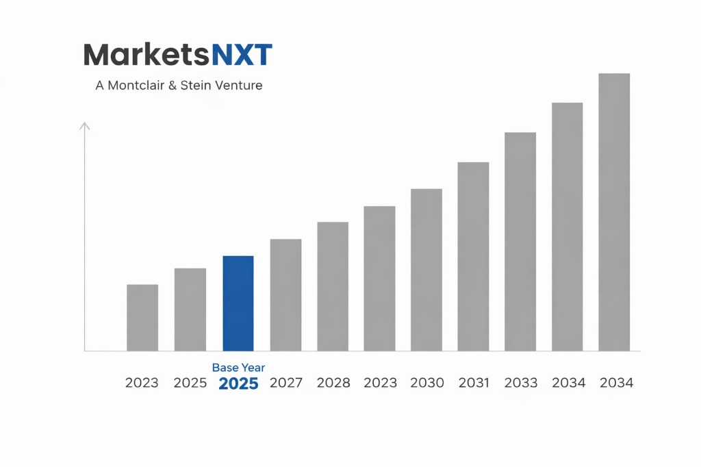
- ✓Market Size 2024: USD 6.8 billion
- ✓Market Size 2032: USD 11.9 billion
- ✓CAGR: 7.2%
- ✓Base Year: 2025
- ✓Forecast Period: 2026–2032
Analyst Recommendation — Dual-Source Gallium Now: Procurement leaders at U.S. compound semiconductor and power device fabs should qualify a second gallium and germanium supplier outside China before the end of 2026. Contracted offtake from Canadian and Australian gallium projects secures volume now.
The United States' Role in the Global Semiconductor Materials Supply Chain
The United States accounts for a modest share of global semiconductor materials output by volume but controls the design-critical layer of consumption. American fabs, led by Intel's Arizona and Ohio projects, TSMC's Phoenix complex and Samsung's Taylor, Texas site, draw on imported photoresists, high-purity gases and wafers. Domestic producers including Entegris, Air Products and Dow supply specialty chemicals, bulk gases and polishing consumables, while wafer and resist production remains concentrated in Japan, Taiwan and South Korea.
Import dependency is highest in wafers and photoresists. Japan remains the largest source of advanced resists and polished silicon wafers reaching U.S. facilities, followed by Taiwan and South Korea, while Germany supplies high-purity quartz ware and precision consumables. The United States is a net exporter of helium and several electronic-grade specialty gases, which gives it leverage in gas-intensive process chemistry. This split makes the country a value-added processing hub downstream and a dependent importer upstream.
Growth Drivers for U.S. Fabrication Materials Trade and Production
The CHIPS and Science Act of 2022 allocated USD 52.7 billion to domestic semiconductor manufacturing, including USD 39 billion in direct manufacturing incentives. Award recipients such as Intel, TSMC, Samsung and Micron are building wafer fabs that require sustained volumes of resists, specialty gases and slurries. Each new leading-edge fab creates recurring materials demand for decades, shifting import volumes toward domestic distribution hubs in Arizona and Texas.
Domestic wafer capacity is expanding in parallel. GlobalWafers is operating its Sherman, Texas wafer plant, and Amkor is building advanced packaging capacity at its Peoria, Arizona campus. Packaging demand for high-bandwidth memory and AI accelerators raises consumption of underfills, substrates and specialty chemicals. This import substitution trend reduces transpacific freight exposure for the packaging supply chain.
Supply Chain Risks and Trade Barriers
Critical mineral dependency is the most acute risk. China imposed export licensing on gallium and germanium in 2023 and banned shipments of both metals to the United States in December 2024. Helium supply has tightened since the sale of the Federal Helium Reserve in 2024, and the 2022 neon disruption exposed how a single regional supplier can halt lithography output within weeks.
Logistics and trade policy add further exposure. Section 301 tariffs on Chinese semiconductors rise to 50 percent in 2025, and a Section 232 investigation into semiconductor imports could widen duties across additional materials categories. Water availability in Arizona constrains ultrapure water production for chemical and wafer processing. A weaker yen raised landed costs for Japanese resists during 2024, exposing fabs to currency swings.
Trade and Investment Opportunities in the United States
Gas and chemical suppliers can pursue on-site supply agreements with the Arizona and Texas fab clusters, where long-term contracts reduce logistics risk and secure dedicated capacity. Domestic production of wet chemicals and high-purity solvents offers a clear import substitution play, since these products currently ship from Asia with lead times of several months. Suppliers that qualify locally early will capture the replacement cycle as fabs ramp.
Foreign direct investment is flowing into materials production alongside fab construction. Japanese and Korean chemical majors have announced U.S. plants to serve domestic customers, and the Gulf Coast offers feedstock access and port infrastructure for specialty chemicals. Logistics hub development in Phoenix and the Houston ship channel can consolidate inbound materials for multiple fabs, reducing inventory carrying costs across the region.
Market at a Glance
| Metric | Value |
|---|---|
| Market Size 2024 | USD 6.8 billion |
| Market Size 2032 | USD 11.9 billion |
| Growth Rate (CAGR) | 7.2% |
| Most Critical Decision Factor | Qualification timelines for advanced-node materials and supplier proximity |
| Largest Region | Southwest (Arizona and Texas) |
| Competitive Structure | Oligopolistic, led by Japanese and U.S. multinationals |
Leading Market Participants
- Entegris
- Air Products and Chemicals
- Linde
- Merck KGaA (EMD Electronics)
- Dow
- Shin-Etsu Chemical
- SUMCO
- GlobalWafers
- Photronics
- DuPont
Regulatory and Trade Policy Environment
The CHIPS and Science Act governs federal incentives, with grant conditions tied to construction milestones and restrictions on expanding advanced manufacturing in designated countries of concern. The advanced manufacturing investment tax credit under Section 48D supports materials-adjacent fab capital spending. Export controls administered by the Bureau of Industry and Security restrict advanced chip and equipment transfers, indirectly shaping which materials suppliers can serve restricted customers.
Tariff and chemical regulation shape import economics. Section 301 duties apply to Chinese semiconductor inputs, while most Japanese and Korean materials enter under normal tariff schedules supported by bilateral trade relationships. The Toxic Substances Control Act requires EPA reporting for fluoropolymers and PFAS used in lithography and etch chemistries, adding compliance cost for chemical suppliers. Free trade agreements with Korea and Japan provide tariff predictability but do not cover critical mineral export controls imposed by third countries.
U.S. Semiconductor Materials Supply Chain Outlook to 2032
Domestic materials capacity will grow fastest in ultrapure chemicals, bulk gases and advanced packaging materials as fabs in Arizona and Texas reach volume production. Photoresist and high-purity wafer production will remain import-dependent through the early 2030s because qualification cycles and capital requirements are long. Import shares for wet chemicals and gases will decline as local plants reach scale.
Technology transitions will shift comparative advantage. High-NA EUV lithography and glass substrates for advanced packaging will favor suppliers with proprietary resist and substrate chemistries, which concentrates bargaining power among a few Japanese and U.S. firms. Compound semiconductor demand for gallium and germanium will push the United States toward recovery projects in Canada and Australia, reshaping sourcing routes away from China over the forecast period.
Market Segmentation
- Photoresists
- Ultrapure Process Gases
- Silicon Wafers
- CMP Slurries and Pads
- Photomasks
- Wet Chemicals
- Front-End Wafer Fabrication
- Lithography
- Deposition and Etch
- Advanced Packaging
- Integrated Device Manufacturers
- Foundries
- Pilot and Research Lines
- OSAT Packaging Houses
- Which countries supply most U.S. semiconductor fabrication materials?
- Japan is the largest source of advanced photoresists and polished wafers, followed by Taiwan and South Korea. Germany supplies quartz ware and precision consumables, while the United States exports helium and several specialty gases.
- How does the CHIPS Act affect materials sourcing?
- The Act funds fab construction, which creates steady demand for resists, gases and slurries in Arizona and Texas. Materials suppliers, however, are expanding more slowly than fabs, so imports remain necessary through the early 2030s.
- What is the main logistics risk for U.S. fab materials?
- Concentrated supply from Japan and Taiwan exposes fabs to shipping disruption and port congestion on the Pacific route. Ultrapure water and chemical shipments also face tight lead times when inventories run low.
- Are gallium and helium shortages a near-term risk?
- China's December 2024 ban on gallium and germanium shipments to the United States creates immediate exposure for compound semiconductor fabs. Helium supply is tighter since the Federal Helium Reserve sale, although domestic production remains significant.
- How long does qualifying a new materials supplier take?
- Qualification of advanced-node materials typically takes 18 to 24 months, including process integration and yield testing. Fabs therefore favor incumbent suppliers, and new entrants must secure early pilot-line commitments.
- Table of Contents
- Chapter 01 Methodology and Scope
- 1.1 Research Methodology
- 1.2 Scope and Definitions
- 1.3 Data Sources
- Chapter 02 Executive Summary
- 2.1 Report Highlights
- 2.2 Market Size and Forecast 2024-2032
- Chapter 03 U.S. Semiconductor Fabrication Materials - Market Analysis
- 3.1 Market Overview
- 3.2 Growth Drivers
- 3.3 Restraints
- 3.4 Opportunities
- Chapter 04 Material Type Insights
- 4.1 Photoresists
- 4.2 Ultrapure Process Gases
- 4.3 Silicon Wafers
- 4.4 CMP Slurries and Pads
- 4.5 Others
- Chapter 05 Process Stage Insights
- 5.1 Front-End Wafer Fabrication
- 5.2 Lithography
- 5.3 Deposition and Etch
- 5.4 Advanced Packaging
- 5.5 Others
- Chapter 06 Fab Ownership Insights
- 6.1 Integrated Device Manufacturers
- 6.2 Foundries
- 6.3 Pilot and Research Lines
- 6.4 OSAT Packaging Houses
- 6.5 Others
- Chapter 07 Competitive Landscape
- 7.1 Market Players
- 7.2 Leading Market Participants
- 7.2.1 Entegris
- 7.2.2 Air Products and Chemicals
- 7.2.3 Linde
- 7.2.4 Merck KGaA (EMD Electronics)
- 7.2.5 Dow
- 7.2.6 Shin-Etsu Chemical
- 7.2.7 SUMCO
- 7.2.8 GlobalWafers
- 7.2.9 Photronics
- 7.2.10 DuPont
- 7.3 Regulatory Environment
- 7.4 Outlook
Table of Contents
Research Framework and Methodological Approach
Information
Procurement
Information
Analysis
Market Formulation
& Validation
Overview of Our Research Process
MarketsNXT follows a structured, multi-stage research framework designed to ensure accuracy, reliability, and strategic relevance of every published study. Our methodology integrates globally accepted research standards with industry best practices in data collection, modeling, verification, and insight generation.
1. Data Acquisition Strategy
Robust data collection is the foundation of our analytical process. MarketsNXT employs a layered sourcing model.
- Company annual reports & SEC filings
- Industry association publications
- Technical journals & white papers
- Government databases (World Bank, OECD)
- Paid commercial databases
- KOL Interviews (CEOs, Marketing Heads)
- Surveys with industry participants
- Distributor & supplier discussions
- End-user feedback loops
- Questionnaires for gap analysis
Analytical Modeling and Insight Development
After collection, datasets are processed and interpreted using multiple analytical techniques to identify baseline market values, demand patterns, growth drivers, constraints, and opportunity clusters.
2. Market Estimation Techniques
MarketsNXT applies multiple estimation pathways to strengthen forecast accuracy.
Bottom-up Approach
Aggregating granular demand data from country level to derive global figures.
Top-down Approach
Breaking down the parent industry market to identify the target serviceable market.
Supply Chain Anchored Forecasting
MarketsNXT integrates value chain intelligence into its forecasting structure to ensure commercial realism and operational alignment.
Supply-Side Evaluation
Revenue and capacity estimates are developed through company financial reviews, product portfolio mapping, benchmarking of competitive positioning, and commercialization tracking.
3. Market Engineering & Validation
Market engineering involves the triangulation of data from multiple sources to minimize errors.
Extensive gathering of raw data.
Statistical regression & trend analysis.
Cross-verification with experts.
Publication of market study.
Client-Centric Research Delivery
MarketsNXT positions research delivery as a collaborative engagement rather than a static information transfer. Analysts work with clients to clarify objectives, interpret findings, and connect insights to strategic decisions.