
U.S. Semiconductor Materials Market Size, Share & Forecast 2026–2032
Report Highlights
- ✓Country: United States
- ✓Market: Semiconductor Materials
- ✓Market Size 2024: USD 9.4 billion
- ✓Market Size 2032: USD 15.6 billion
- ✓CAGR: 6.5%
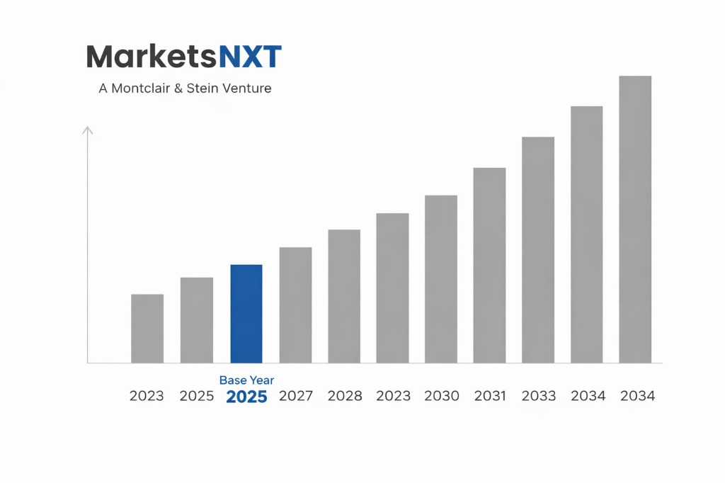
- ✓Base Year: 2025
- ✓Forecast Period: 2026–2032
Analyst Recommendation — Lock Gallium Offtake Now: Buyers at U.S. compound semiconductor and fab operators should secure multi-year gallium and germanium offtake agreements with non-Chinese suppliers before Q4 2026. License-dependent Chinese supply is tightening, and contracts signed later will carry premium pricing.
Semiconductor Materials in the U.S.: Market Overview
The U.S. semiconductor materials market was valued at USD 9.4 billion in 2024 and will reach USD 15.6 billion by 2032. Materials cover silicon wafers, photoresists, specialty gases, CMP slurries, and high-purity chemicals sold into wafer fabrication, packaging, and test. Demand is concentrated in logic, memory, and advanced packaging, and the 6.5% CAGR reflects fab construction rather than consumption alone. Domestic fab output has grown faster than domestic materials production, so the market remains import-dependent for most critical chemistries.
Policy has moved this market from a private, import-led structure to a state-directed build-out. Entegris, Air Products, and Linde supplied the earlier domestic base from plants in Massachusetts and Pennsylvania, but the CHIPS and Science Act of 2022 made the Department of Commerce the largest source of new capital for materials capacity. Government leads on capital and export controls, while private firms still control chemistry, qualification, and product innovation.
Policy-Driven Growth in U.S. Semiconductor Materials
The CHIPS and Science Act of 2022 (Public Law 117-167) authorizes USD 39 billion in manufacturing incentives, administered by the Commerce Department's CHIPS Program Office. Award recipients such as GlobalWafers, which is building a wafer plant in Sherman, Texas, must source materials domestically to meet capacity commitments. Every awarded fab creates long-term demand for wafers, gases, and chemicals, transmitting subsidy directly into materials volumes.
The Advanced Manufacturing Investment Credit under Section 48D of the Internal Revenue Code provides a 35% tax credit on qualified fab investment, following the One Big Beautiful Bill Act of 2025, for construction beginning before January 1, 2027. This deadline makes new fab construction economic and pulls materials demand forward into 2026 and 2027. Separately, Defense Production Act Title III funding, administered by the Department of Defense, supports domestic gallium and germanium recovery so that defense-grade chip materials are not sourced solely abroad.
Regulatory Barriers and Compliance Costs
Export controls administered by the Bureau of Industry and Security under the Export Administration Regulations restrict the sale of advanced materials and equipment to China. License applications carry a standard review window of up to 90 days, delaying shipments of specialty materials to Chinese customers. Exporters must screen every end user against the Entity List and retain transaction records for five years.
The Toxic Substances Control Act, administered by the Environmental Protection Agency, imposes PFAS reporting obligations under section 8(a)(7) on manufacturers and importers of fluorinated chemicals, which include many etchants and photoresist components. Section 301 tariffs administered by the U.S. Trade Representative raised duties on Chinese semiconductors to 50% from January 2025, increasing landed costs for imported wafers and materials. CHIPS award recipients also face a ten-year restriction on expanding advanced capacity in countries of concern.
Policy-Created Opportunities in the U.S.
The National Advanced Packaging Manufacturing Program, funded at USD 1.4 billion under the CHIPS Act and run through NIST, creates demand for substrates, underfill, and dielectric materials used in advanced packaging. Suppliers qualifying products for 2.5D and 3D packaging lines gain early access to programme-funded pilot lines. Packaging chemistry remains a segment where domestic qualification is thin, and suppliers should target Natcast, which operates the National Semiconductor Technology Center, to secure qualification partnerships.
The Department of Defense Microelectronics Commons, operating eight regional hubs, funds prototype materials and process development for defense applications. Gallium nitride and silicon carbide substrates for radar and power electronics face sourcing requirements under the Defense Federal Acquisition Regulation Supplement, favoring domestic suppliers. Early qualification under these rules secures long-term contracts and insulates pricing as Chinese-sourced materials face license restrictions.
Market at a Glance
| Metric | Value |
|---|---|
| Market Size 2024 | USD 9.4 billion |
| Market Size 2032 | USD 15.6 billion |
| Growth Rate (CAGR) | 6.5% |
| Most Critical Decision Factor | Secured access to gallium, germanium, and qualified photoresist supply |
| Largest Region | Southwest (Arizona and Texas fab clusters) |
| Competitive Structure | Concentrated oligopoly led by foreign-owned suppliers |
Leading Market Participants
- Entegris
- Air Products
- Linde
- Merck KGaA
- Shin-Etsu Chemical
- GlobalWafers
- Hemlock Semiconductor
- Resonac
- DuPont
- Fujifilm Electronic Materials
Regulatory and Policy Environment
The primary legislation is the CHIPS and Science Act of 2022 (Public Law 117-167), with manufacturing incentives administered by the Commerce Department's CHIPS Program Office and research programmes run by NIST. Recipients must comply with a ten-year guardrail on expanding advanced manufacturing in countries of concern, alongside workforce and environmental plans. Export controls operate under the Export Control Reform Act of 2018, enforced by the Bureau of Industry and Security.
Upcoming changes include the TSCA PFAS reporting window, scheduled to open in 2026 under EPA's section 8(a)(7) rule, and the Section 232 investigation into semiconductor imports launched in April 2025, whose tariff outcome remains pending. Section 48D construction must begin before January 1, 2027. Compared with regional peers, the U.S. framework relies on tax credits and grants, whereas the EU Chips Act under Regulation (EU) 2023/1781 uses a coordinated governance model and Japan's Economic Security Promotion Act directs subsidies toward domestic supply chains.
Long-Term Policy Outlook for U.S. Semiconductor Materials
By 2032, export controls will extend from finished chips to specialty materials, with the Bureau of Industry and Security expanding controls on gallium, germanium, and high-purity precursors. Domestic capacity from CHIPS-funded plants will shift the import mix toward U.S.-produced wafers and gases, but photoresists will remain import-reliant. Tariff policy under Section 232 and Section 301 will set the cost of imported chemistries, pushing Japanese suppliers to localize final-stage production.
The Section 48D construction deadline will produce a 2026 to 2027 demand peak, followed by a normalizing materials market growing near 6.5% annually as fabs enter steady-state operation. Policy will shift from subsidy toward sustainment, with the CHIPS Program Office focusing on fab utilization, while TSCA compliance costs rise for fluorinated chemical users. Suppliers that secure qualification before 2028 will hold share through 2032.
Frequently Asked Questions
Market Segmentation
- Silicon Wafers
- Photoresists and Chemicals
- Specialty Gases
- CMP Slurries and Pads
- Sputtering Targets
- Logic
- Memory
- Analog and Power
- Advanced Packaging
- Foundries
- Integrated Device Manufacturers
- Outsourced Assembly and Test Providers
- Defense Microelectronics
Table of Contents
Research Framework and Methodological Approach
Information
Procurement
Information
Analysis
Market Formulation
& Validation
Overview of Our Research Process
MarketsNXT follows a structured, multi-stage research framework designed to ensure accuracy, reliability, and strategic relevance of every published study. Our methodology integrates globally accepted research standards with industry best practices in data collection, modeling, verification, and insight generation.
1. Data Acquisition Strategy
Robust data collection is the foundation of our analytical process. MarketsNXT employs a layered sourcing model.
- Company annual reports & SEC filings
- Industry association publications
- Technical journals & white papers
- Government databases (World Bank, OECD)
- Paid commercial databases
- KOL Interviews (CEOs, Marketing Heads)
- Surveys with industry participants
- Distributor & supplier discussions
- End-user feedback loops
- Questionnaires for gap analysis
Analytical Modeling and Insight Development
After collection, datasets are processed and interpreted using multiple analytical techniques to identify baseline market values, demand patterns, growth drivers, constraints, and opportunity clusters.
2. Market Estimation Techniques
MarketsNXT applies multiple estimation pathways to strengthen forecast accuracy.
Bottom-up Approach
Aggregating granular demand data from country level to derive global figures.
Top-down Approach
Breaking down the parent industry market to identify the target serviceable market.
Supply Chain Anchored Forecasting
MarketsNXT integrates value chain intelligence into its forecasting structure to ensure commercial realism and operational alignment.
Supply-Side Evaluation
Revenue and capacity estimates are developed through company financial reviews, product portfolio mapping, benchmarking of competitive positioning, and commercialization tracking.
3. Market Engineering & Validation
Market engineering involves the triangulation of data from multiple sources to minimize errors.
Extensive gathering of raw data.
Statistical regression & trend analysis.
Cross-verification with experts.
Publication of market study.
Client-Centric Research Delivery
MarketsNXT positions research delivery as a collaborative engagement rather than a static information transfer. Analysts work with clients to clarify objectives, interpret findings, and connect insights to strategic decisions.