Non-UV Dicing Tape Market Size, Share & Forecast 2026–2034
Report Highlights
- ✓Market Size 2024: USD 312.4 million
- ✓Market Size 2034: USD 581.7 million
- ✓CAGR: 6.4%
- ✓Market Definition: Non-UV dicing tapes are pressure-sensitive adhesive films used to secure semiconductor wafers during the dicing process without requiring ultraviolet light for release. They serve applications where UV exposure is incompatible with sensitive device materials or downstream process requirements.
- ✓Leading Companies: Nitto Denko, Lintec Corporation, Sumitomo Bakelite, AI Technology, Furukawa Electric
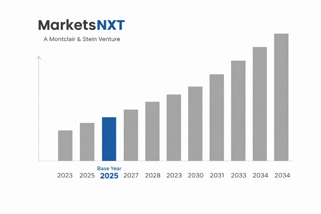
- ✓Base Year: 2025
- ✓Forecast Period: 2026–2034
Analyst Recommendation — Enter SiC Supply Chain Now: Adhesive tape manufacturers and specialty chemical suppliers must secure qualification slots with Tier-1 SiC wafer producers — specifically Wolfspeed and onsemi — before 2026. Qualification cycles run 18–24 months, and late entrants will be locked out of the highest-margin EV-related volume for the entire forecast period.
Non-UV dicing tape at a turning point: Market Overview
The global non-UV dicing tape market was valued at USD 312.4 million in 2024 and is forecast to reach USD 581.7 million by 2034, expanding at a CAGR of 6.4%. The market occupies a specific but increasingly critical niche within the broader semiconductor packaging materials ecosystem. Non-UV tapes use thermal, mechanical, or water-soluble release mechanisms rather than ultraviolet photon activation, making them indispensable for device types where UV exposure degrades performance, distorts delicate structures, or conflicts with process flow. Historically positioned as a secondary format to UV-release tapes, the segment is now gaining structural importance as wafer material diversity expands beyond traditional silicon.
The current turning point is driven by two concurrent shifts: the rapid proliferation of wide-bandgap semiconductor materials — principally silicon carbide and gallium nitride — and the increasing adoption of advanced wafer-level packaging architectures that embed sensitive optical or photonic components. Both trends make UV-based release chemistry problematic or entirely unusable. Simultaneously, compound semiconductor fabs in South Korea, Japan, and Taiwan are upgrading capacity specifically for EV power electronics and 5G RF chips, generating fresh procurement cycles for non-UV compatible process consumables. This is not incremental demand; it represents a structural reallocation of tape specification requirements at the process engineering level.
Key forces shaping non-UV dicing tape growth
The primary growth force is the SiC wafer production ramp for electric vehicle power modules. SiC's physical hardness and optical transmission characteristics make UV-activated adhesive release geometrically unreliable — energy absorption is uneven across the wafer surface, causing partial release failures and yield loss. Non-UV thermal-release tapes eliminate this variability entirely. As global SiC wafer capacity is projected to more than triple between 2024 and 2028 — led by investments from Wolfspeed in North Carolina, STMicroelectronics in Catania, and Infineon in Kulim — procurement volumes for compatible dicing consumables are scaling in direct proportion, benefiting the non-UV segment specifically and disproportionately.
The second growth force is the expansion of photonic integrated circuit and optical sensor manufacturing, where UV light during the dicing stage would activate photodetectors or alter waveguide material properties. This application segment is growing at above-market rates in Taiwan and China, anchored by TSMC's photonics program and domestic Chinese foundry investment. A third force is the rise of temporary wafer bonding processes in advanced fan-out packaging, where UV-transparent carrier substrates make UV-release tapes geometrically incompatible. Each of these forces channels demand specifically into non-UV formats, creating compounding revenue tailwinds across the materials supply chain that run independently of each other.
Barriers and risks in the non-UV dicing tape market
The most consequential structural barrier is the technical complexity of formulating non-UV release adhesives that match the peel-force consistency, die-attach cleanliness, and thermal budget compatibility demanded by leading-edge fabs. UV-release tapes benefit from a larger, more mature supplier base and deeper process engineering documentation. Non-UV alternatives — particularly thermally released formats — require tighter adhesive coating uniformity tolerances and more precisely controlled oven integration in the dicing line. Achieving the sub-5-micron kerf contamination thresholds required for SiC device dicing pushes formulation costs significantly higher, creating a barrier that favors established Japanese chemical firms over emerging competitors and suppresses margin expansion even as volumes grow.
The primary cyclical risk is a slowdown in EV production and SiC capacity investment. The SiC supply chain has experienced inventory normalization pressures through late 2024, and if EV adoption rates undershoot projections in Europe and China — the two most SiC-intensive vehicle markets — capacity expansion timelines will be extended or deferred, directly reducing dicing tape qualification volumes. This risk is more dangerous than the structural barrier because it is externally driven and can materialize quickly. A 15% reduction in forecast SiC wafer output in 2026 would eliminate an estimated USD 18–22 million in non-UV tape demand that is already priced into current supplier revenue models.
Emerging opportunities in non-UV dicing tape
The most immediately actionable emerging opportunity is the qualification of non-UV tapes for gallium oxide and indium phosphide device wafers — next-generation wide-bandgap materials currently transitioning from research to early production at specialty fabs in the United States, Germany, and Japan. These materials are even more UV-sensitive than SiC, and no large-volume dicing tape supplier has achieved comprehensive qualification across all substrate orientations as of early 2025. The first supplier to achieve full InP and Ga2O3 qualification with two or more Tier-1 foundries before end-2026 will establish a defensible first-mover position in a segment projected to reach significant commercial scale by 2029.
A second near-term opportunity exists in the replacement of solvent-based dicing tapes in China's domestic semiconductor supply chain. Under technology export restriction pressures, Chinese fabs are actively substituting imported UV-release tapes with domestically sourced alternatives — and non-UV water-soluble and thermal-release formats are being evaluated as simultaneously domestic and technically superior for the compound semiconductor lines being built. Companies including Suzhou Boyi and Beijing Tongmei are positioned to benefit, but the condition for market materialization is continued tightening of US export controls, which makes this opportunity policy-contingent rather than purely technology-driven. The policy trajectory supports it clearly through 2027.
Investment Case: Bull, Bear, and What Decides It
The bull case rests on three simultaneous conditions executing as planned: SiC wafer capacity expansions by Wolfspeed, STMicroelectronics, and Onsemi proceed on schedule through 2027; photonic IC manufacturing in Taiwan scales at the rate TSMC's roadmap implies; and Chinese domestic semiconductor buildout accelerates non-UV tape localization. Under these conditions, non-UV dicing tape demand grows at 8–9% annually in volume terms from 2026 onward, and the premium pricing that thermal-release and water-soluble formats command over standard UV tapes is maintained. The total addressable market for non-UV formats reaches 28–30% of all dicing tape revenue globally by 2030, up from roughly 18% today.
The bear case activates if EV demand softens materially in 2026–2027, causing SiC producers to delay capacity additions and reduce dicing consumable qualification orders. Simultaneously, if TSMC's photonics timeline slips by 18 or more months — a credible risk given integration complexity — the photonic IC demand pull disappears from near-term procurement. In this scenario, non-UV tape demand reverts to its historical growth rate of 3–4%, largely driven by legacy compound semiconductor maintenance volumes. Suppliers who have invested in SiC-specific formulation R&D will face underutilized development cost amortization, compressing margins through 2028 without corresponding revenue growth to offset the investment.
The swing variable is SiC wafer output volume in 2026. If global SiC wafer shipments exceed 2.5 million 150mm-equivalent units in 2026 — the threshold at which dicing tape procurement scales from qualification lots to full production volumes — the bull case is confirmed and supply chain positioning becomes the dominant competitive dynamic. If shipments fall below 1.8 million units due to EV demand misses or fab ramp delays, the bear case dominates through at least 2027. This single metric, reportable quarterly through Wolfspeed and STMicroelectronics earnings disclosures, is the number every participant in this market must track above all others.
Market at a Glance
| Metric | Detail |
|---|---|
| Market Size 2024 | USD 312.4 million |
| Market Size 2034 | USD 581.7 million |
| Growth Rate (CAGR) | 6.4% |
| Most Critical Decision Factor | SiC wafer production volume trajectory through 2027 |
| Largest Region | Asia Pacific |
| Competitive Structure | Concentrated — top 3 Japanese suppliers hold majority share |
Regional performance: Where non-UV dicing tape is growing fastest
Asia Pacific is the largest revenue-contributing region, accounting for over 62% of global non-UV dicing tape consumption in 2024, anchored by Japan's advanced material dicing operations, Taiwan's photonic and RF semiconductor fabs, and South Korea's compound semiconductor investment cycle. Japan holds the deepest technical relationship between tape suppliers and device manufacturers — Nitto Denko and Lintec Corporation supply directly into co-development programs with Japanese SiC device producers including Rohm and Mitsubishi Electric. Taiwan's growth rate within the region is accelerating fastest, driven by TSMC's photonics program and the expansion of compound semiconductor outsourced assembly and test capacity in the Hsinchu corridor.
North America is the second-largest region and the fastest-growing outside Asia, driven primarily by Wolfspeed's Mohawk Valley SiC fab in Marcy, New York, and the broader domestic semiconductor manufacturing push incentivized by the CHIPS Act. European demand is growing steadily, anchored by STMicroelectronics in Catania and Infineon's Kulim-adjacent European operations, as both firms are major SiC power module producers with increasing non-UV tape procurement requirements. Latin America and the Middle East and Africa together contribute less than 4% of global revenue and remain distribution-dependent markets with no indigenous semiconductor wafer fabrication currently driving direct demand for specialty dicing consumables. The North America growth trajectory is the most important regional variable for the 2026–2028 period.
Leading Market Participants
- Nitto Denko Corporation
- Lintec Corporation
- Sumitomo Bakelite Co., Ltd.
- Furukawa Electric Co., Ltd.
- AI Technology, Inc.
- Mitsui Chemicals Tohcello, Inc.
- Denka Company Limited
- Shin-Etsu Chemical Co., Ltd.
- Suzhou Boyi Semiconductor Material Co., Ltd.
- Toyo Adtec Inc.
Where is non-UV dicing tape headed by 2034
By 2034, the non-UV dicing tape market will be a USD 581.7 million segment with a materially different application profile than today. Wide-bandgap semiconductor dicing — SiC, GaN, and emerging gallium oxide — will account for an estimated 45% of total demand, displacing the current dominance of legacy silicon and standard compound semiconductor applications. The competitive structure will remain concentrated, with Japanese chemical manufacturers retaining the majority of high-value SiC and photonic-application share, but Chinese domestic suppliers will have captured a structurally significant share of that country's internal consumption, particularly in the thermal-release sub-segment where localization is technically achievable within the forecast horizon.
Nitto Denko and Lintec Corporation are best positioned for 2034 because both have active co-development programs with leading SiC device producers and have invested in thermal-release formulation R&D specifically for wide-bandgap substrates. Their qualification depth at Tier-1 fabs creates switching cost moats that will persist for most of the forecast period. Sumitomo Bakelite is well-positioned in the photonic IC tape segment. The companies most at risk are mid-tier distributors and formulators without direct fab qualification relationships, as the market's shift toward application-specific formulations will erode the viability of general-purpose non-UV tape products that currently serve legacy markets at competitive price points.
Market Segmentation
By Release Mechanism
- Thermal Release
- Water-Soluble Release
- Mechanical Release
- Chemical Release
By Substrate Material
- Silicon Carbide (SiC)
- Gallium Nitride (GaN)
- Indium Phosphide (InP)
- Silicon
- Gallium Arsenide (GaAs)
- Others
By Application
- Power Semiconductors
- RF and Microwave Devices
- Photonic Integrated Circuits
- MEMS Devices
- LED Components
- Others
By End-Use Industry
- Automotive and EV
- Consumer Electronics
- Telecommunications
- Industrial Automation
- Aerospace and Defense
Frequently Asked Questions
SiC's optical transmission and surface hardness cause uneven UV energy absorption, producing inconsistent adhesive release and elevated die-loss rates. Thermal-release non-UV tapes deliver uniform, repeatable release forces independent of substrate optical properties, making them the process-qualified choice for SiC production lines.
Nitto Denko and Lintec Corporation hold the strongest positions, anchored by co-development qualification relationships with leading SiC and GaN device producers in Japan and Taiwan. Their formulation depth in thermal-release chemistry is not replicable quickly by challengers without multi-year fab qualification programs.
SiC wafer shipment volumes reported by Wolfspeed and STMicroelectronics in their quarterly earnings are the single most informative leading indicator for non-UV tape demand trajectory. Any revision to SiC production ramp guidance from these two producers directly reprices the growth outlook for dicing tape suppliers.
CHIPS Act funding is accelerating SiC and compound semiconductor fab construction in the United States, with Wolfspeed's Mohawk Valley facility the most directly relevant project. Domestic fab qualification requirements create new non-UV tape procurement cycles that were structurally absent from the North American market before 2023.
Consolidation among mid-tier non-UV tape formulators is likely before 2030, as the shift to application-specific SiC and photonic formulations raises the R&D cost baseline beyond what smaller generalist suppliers can sustain. The most probable consolidation path is acquisition of qualified niche formulators by Nitto Denko or Sumitomo Bakelite to accelerate portfolio expansion.
Frequently Asked Questions
Market Segmentation
- Thermal Release
- Water-Soluble Release
- Mechanical Release
- Chemical Release
- Silicon Carbide (SiC)
- Gallium Nitride (GaN)
- Indium Phosphide (InP)
- Silicon
- Gallium Arsenide (GaAs)
- Others
- Power Semiconductors
- RF and Microwave Devices
- Photonic Integrated Circuits
- MEMS Devices
- LED Components
- Others
- Automotive and EV
- Consumer Electronics
- Telecommunications
- Industrial Automation
- Aerospace and Defense
Table of Contents
Research Framework and Methodological Approach
Information
Procurement
Information
Analysis
Market Formulation
& Validation
Overview of Our Research Process
MarketsNXT follows a structured, multi-stage research framework designed to ensure accuracy, reliability, and strategic relevance of every published study. Our methodology integrates globally accepted research standards with industry best practices in data collection, modeling, verification, and insight generation.
1. Data Acquisition Strategy
Robust data collection is the foundation of our analytical process. MarketsNXT employs a layered sourcing model.
- Company annual reports & SEC filings
- Industry association publications
- Technical journals & white papers
- Government databases (World Bank, OECD)
- Paid commercial databases
- KOL Interviews (CEOs, Marketing Heads)
- Surveys with industry participants
- Distributor & supplier discussions
- End-user feedback loops
- Questionnaires for gap analysis
Analytical Modeling and Insight Development
After collection, datasets are processed and interpreted using multiple analytical techniques to identify baseline market values, demand patterns, growth drivers, constraints, and opportunity clusters.
2. Market Estimation Techniques
MarketsNXT applies multiple estimation pathways to strengthen forecast accuracy.
Bottom-up Approach
Aggregating granular demand data from country level to derive global figures.
Top-down Approach
Breaking down the parent industry market to identify the target serviceable market.
Supply Chain Anchored Forecasting
MarketsNXT integrates value chain intelligence into its forecasting structure to ensure commercial realism and operational alignment.
Supply-Side Evaluation
Revenue and capacity estimates are developed through company financial reviews, product portfolio mapping, benchmarking of competitive positioning, and commercialization tracking.
3. Market Engineering & Validation
Market engineering involves the triangulation of data from multiple sources to minimize errors.
Extensive gathering of raw data.
Statistical regression & trend analysis.
Cross-verification with experts.
Publication of market study.
Client-Centric Research Delivery
MarketsNXT positions research delivery as a collaborative engagement rather than a static information transfer. Analysts work with clients to clarify objectives, interpret findings, and connect insights to strategic decisions.