Wafer Dicing Saws Market Size, Share & Forecast 2026–2034
Report Highlights
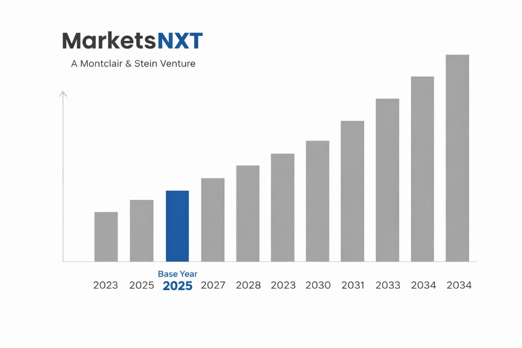
- ✓Market Size 2024: USD 1.82 billion
- ✓Market Size 2034: USD 3.41 billion
- ✓CAGR: 6.5%
- ✓Market Definition: Wafer dicing saws are precision cutting systems used to singulate semiconductor wafers into individual dies using blade, laser, or plasma dicing methods. The market encompasses equipment, consumable blades, and associated dicing process services for semiconductor and electronics manufacturing.
- ✓Leading Companies: DISCO Corporation, Tokyo Seimitsu, Kulicke and Soffa, ACCRETECH, Advanced Dicing Technologies
- ✓Base Year: 2025
- ✓Forecast Period: 2026–2034
Analyst Recommendation — Enter Consumables, Not Equipment: Investors and suppliers targeting this market must prioritise the blade consumables segment over capital equipment. Secure long-term supply agreements with tier-one OSATs in Southeast Asia by end of 2026 to capture recurring revenue streams insulated from equipment replacement cycles.
Wafer dicing saws at a turning point: Market Overview
The global wafer dicing saws market is valued at USD 1.82 billion in 2024, underpinned by sustained capital investment across semiconductor front-end and back-end manufacturing. The market has tracked closely with wafer starts data, expanding at a compounded pace driven by the proliferation of advanced packaging formats, automotive semiconductors, and compound semiconductor devices. DISCO Corporation remains the dominant equipment supplier, commanding a structurally entrenched position reinforced by its consumables ecosystem. The market encompasses precision blade dicing, laser dicing, and plasma dicing systems, with blade dicing commanding the largest installed base across logic, memory, and compound semiconductor fabs globally.
The current moment represents a genuine inflection for wafer dicing saws, driven by two converging structural shifts. First, the transition to heterogeneous integration and chiplet-based architectures demands finer singulation tolerances and reduced kerf widths, pushing equipment specifications beyond the capabilities of legacy dicing platforms. Second, the rapid expansion of silicon carbide wafer production for electric vehicle power modules is generating incremental demand for specialised hard-material dicing systems, a segment where tooling margins are substantially higher than standard silicon. These two forces together are reshaping the product roadmap, competitive positioning, and geographic demand profile of this market in ways that will persist well beyond cyclical semiconductor corrections.
Key forces shaping wafer dicing saw growth
Three specific forces are driving revenue expansion in this market. First, the global EV transition is generating direct demand for silicon carbide dicing solutions. SiC wafer production is forecast to grow at double-digit rates through 2030, with Wolfspeed, STMicroelectronics, and Infineon all commissioning new capacity. SiC's extreme hardness requires specialised diamond blade tooling and modified dicing parameters, creating a premium consumables and equipment replacement cycle that generates higher average selling prices than standard silicon dicing. This force benefits equipment suppliers with dedicated SiC process libraries and application engineering depth, most notably DISCO and Tokyo Seimitsu.
Second, the structural expansion of advanced packaging — including fan-out wafer-level packaging, 2.5D interposers, and through-silicon via integration — requires dicing precision at sub-10-micron tolerances. This drives upgrade cycles at OSAT facilities including ASE Group and Amkor, as legacy blade dicing systems cannot consistently achieve the required die strength and kerf quality at these geometries. Third, geopolitical semiconductor self-sufficiency programs in China, Europe, and the United States are funding greenfield fab construction that mandates fresh capital equipment procurement, directly expanding the addressable installed base for new dicing systems across all three regions simultaneously.
Barriers and risks in the wafer dicing saw market
The primary structural risk is DISCO Corporation's near-monopolistic grip on the market. A supplier concentration of this magnitude creates systemic fragility: any disruption to DISCO's supply chain — whether from Japanese export controls, natural disaster, or component shortage — propagates directly to global semiconductor back-end operations with minimal alternative sourcing. For competitors attempting to gain market share, DISCO's installed base lock-in through proprietary blade specifications and process recipes constitutes a durable structural barrier that cannot be overcome within a single product generation cycle. This is not a cyclical condition; it is the market's defining structural feature and the most dangerous risk to downstream customers.
The primary cyclical risk is semiconductor inventory correction. The 2022–2023 memory downturn demonstrated how rapidly wafer start reductions translate into deferred capital equipment purchases, with DISCO reporting order intake declines exceeding 30% during peak correction periods. Advanced packaging spending is more resilient than memory capex, but it is not immune. A sustained slowdown in AI accelerator demand — the primary current driver of advanced packaging investment — would compress equipment order books within two quarters. Overcapacity in mature-node fabs in China also threatens blade consumable pricing as domestic Chinese competitors including Shenyang Tiantong Laser scale production of lower-cost tooling, eroding margins in the commoditised segment of the consumables market.
Emerging opportunities in wafer dicing saws
The most immediate emerging opportunity is plasma dicing for ultra-thin wafer singulation. As advanced packaging nodes push die thickness below 50 microns, blade and laser dicing introduce unacceptable chipping and microcracking rates. Plasma dicing, commercialised by Orbotech (now part of KLA) and Panasonic Factory Solutions, eliminates mechanical stress entirely and enables simultaneous dicing of entire wafer surfaces. This technology is still sub-5% of total dicing revenue but is positioned for rapid adoption in high-density fan-out packaging and mobile application processor manufacturing. The condition for materialisation is straightforward: cost-per-die parity with laser dicing must be demonstrated at volume, which two major OSATs are currently qualifying in pilot lines.
A second near-term opportunity lies in serving China's domestic semiconductor equipment substitution drive. Beijing's push to replace foreign equipment across the semiconductor supply chain has created funded demand for domestic wafer dicing saw manufacturers, with companies including Shenyang Tiantong Laser and Wuhan Dr Laser Technology receiving state-backed procurement commitments. Foreign suppliers willing to establish local joint ventures or technology licensing arrangements before 2027 can capture engineering service revenue and consumables supply relationships that persist even if equipment sales face restriction. The condition for this opportunity is regulatory: continued US and Japanese export control escalation will accelerate Chinese procurement of domestic or partnership-based alternatives, not eliminate the capital expenditure.
Investment case: bull, bear, and what decides it
The bull case for wafer dicing saws rests on three compounding catalysts that are already in motion. AI infrastructure buildout is sustaining advanced packaging demand at TSMC's CoWoS and Samsung's 2.5D platforms, directly driving OSAT equipment refresh cycles. SiC power device capacity additions at Wolfspeed's Siler City fab and ST's Catania plant are generating incremental hard-material dicing demand with above-market equipment ASPs. Simultaneously, greenfield semiconductor investments under the US CHIPS Act and EU Chips Act are creating net-new installed base demand rather than replacement cycles, which historically yields the highest equipment revenue per programme. Under this scenario, the market comfortably reaches USD 3.41 billion by 2034, with DISCO and Tokyo Seimitsu capturing disproportionate share of the premium equipment segment.
The bear case hinges on demand concentration risk materialising simultaneously across two vectors. If AI accelerator demand plateaus in 2025–2026 due to hyperscaler capex rationalisation — a risk flagged by both Intel Foundry and TSMC in recent investor communications — advanced packaging equipment orders deflate faster than the broader semiconductor cycle. Concurrently, if Chinese domestic equipment suppliers reach acceptable yield performance on standard silicon dicing within three years, the addressable market for foreign blade systems in China — currently a significant consumables revenue base — contracts structurally, not cyclically. Combined, these two forces create a scenario where revenue growth stalls below 4% CAGR and DISCO's premium pricing power erodes at the margin.
The swing variable is advanced packaging volume at TSMC. TSMC's CoWoS and SoIC capacity expansion plans are the single most important demand signal for the wafer dicing saws market because they directly determine OSAT capex commitments, chiplet format standardisation timelines, and the pace of ultra-thin wafer dicing adoption. If TSMC executes its announced CoWoS capacity tripling through 2026, the bull case is confirmed and capital equipment order books will reflect it by Q3 2025. If CoWoS expansion slips by more than two quarters, the bear case gains traction. This is the one data point every participant in this market must track above all others.
Market at a Glance
| Metric | Detail |
|---|---|
| Market Size 2024 | USD 1.82 billion |
| Market Size 2034 | USD 3.41 billion |
| Growth Rate (CAGR) | 6.5% |
| Most Critical Decision Factor | Advanced packaging volume commitments at TSMC CoWoS |
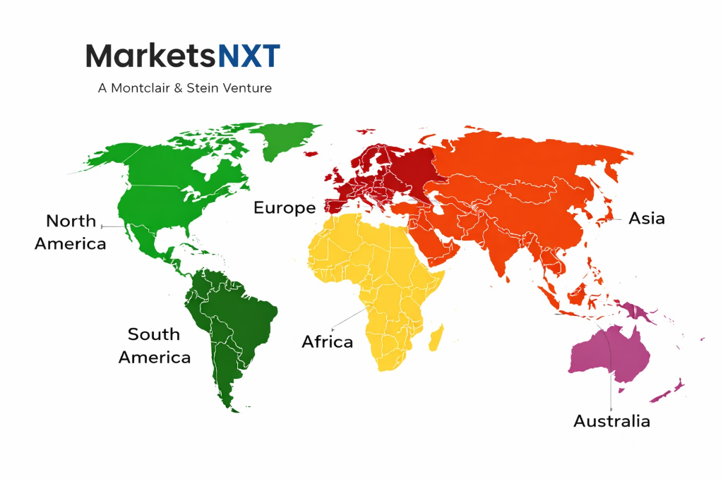
| Largest Region | Asia Pacific |
| Competitive Structure | Near-monopoly with DISCO Corporation dominating equipment share |
Regional performance: where wafer dicing saws are growing fastest
Asia Pacific is the largest revenue contributor by a substantial margin, accounting for the preponderance of global wafer dicing saw demand due to the concentration of semiconductor back-end manufacturing in Taiwan, South Korea, Japan, and increasingly Southeast Asia. Taiwan alone — home to TSMC, ASE Group, and MediaTek's design-driven OSAT relationships — generates the highest density of advanced packaging equipment demand globally. South Korea's Samsung and SK Hynix are investing heavily in HBM memory packaging, which requires precision dicing at reduced kerf widths, sustaining premium equipment demand. Japan remains critical as both a production hub and the home geography of DISCO and Tokyo Seimitsu, where domestic procurement relationships reinforce equipment placement rates.
China represents the highest growth rate among all regions, driven by state-funded semiconductor self-sufficiency investments under the Made in China 2025 and subsequent programmes. New fab construction in cities including Wuhan, Chengdu, and Xi'an is generating equipment demand that partially offsets export control headwinds on leading-edge tools. North America is experiencing a renaissance in fab construction driven by CHIPS Act incentives, with Intel's Ohio and Arizona expansions and TSMC's Phoenix facility creating demand for back-end dicing infrastructure that was largely absent from the US market for two decades. Europe's growth is anchored in SiC and compound semiconductor manufacturing expansion in Germany and Italy, where automotive-grade power device production is scaling aggressively through 2028.
Leading Market Participants
- DISCO Corporation
- Tokyo Seimitsu Co., Ltd. (ACCRETECH)
- Kulicke and Soffa Industries
- Advanced Dicing Technologies (ADT)
- Panasonic Factory Solutions
- CETC Electronics Equipment Group
- Shenyang Tiantong Laser Technology
- Wuhan Dr Laser Technology
- GL Sciences
- Dynatex International
Where wafer dicing saws are headed by 2034
By 2034, the wafer dicing saws market will reach USD 3.41 billion and exhibit greater technology segmentation than today's blade-dominated landscape. Plasma dicing will account for a meaningfully larger share of advanced packaging singulation processes, while laser dicing will be the primary method for compound semiconductors thinner than 100 microns. Blade dicing will persist as the volume workhorse for standard silicon, but competitive pressure on blade consumable pricing will intensify as Chinese domestic tooling manufacturers achieve acceptable quality thresholds. The overall market structure will remain concentrated at the equipment level, with DISCO retaining its leadership position, but consumables competition will fragment across a larger supplier base than exists today.
DISCO Corporation and Tokyo Seimitsu are best positioned for 2034 because their application engineering infrastructure, process recipe libraries, and direct relationships with tier-one OSAT customers create switching costs that no new entrant can replicate within the forecast period. DISCO's investment in plasma dicing and stealth laser dicing platforms positions it to capture the premium segments driving above-average revenue growth. Kulicke and Soffa, with its expanding advanced packaging equipment portfolio, is the most credible challenger to displace incumbents in specific niche segments. Chinese domestic players will capture incremental share within China but are unlikely to threaten the premium global market before 2034 given existing process qualification gaps at advanced packaging nodes.
Market Segmentation
By Dicing Method
- Blade Dicing
- Laser Dicing
- Plasma Dicing
- Stealth Dicing
- Mechanical Scribing
By Wafer Material
- Silicon
- Silicon Carbide (SiC)
- Gallium Nitride (GaN)
- Gallium Arsenide (GaAs)
- Lithium Niobate
- Sapphire
By Application
- Logic Semiconductors
- Memory Devices
- Power Devices
- MEMS
- Optoelectronics
- RF Devices
By End-Use Industry
- Consumer Electronics
- Automotive
- Telecommunications
- Industrial Electronics
- Aerospace and Defense
- Medical Devices
Frequently Asked Questions
Advanced packaging volume at TSMC's CoWoS and SoIC platforms is the most important driver, as it directly determines OSAT capex commitments and equipment refresh cycles. AI accelerator chiplet adoption is the primary mechanism sustaining this demand.
DISCO's dominance stems from proprietary blade specifications, process recipe lock-in, and decades of application engineering relationships with tier-one customers including TSMC and ASE Group. No competitor has replicated this integrated equipment-consumables ecosystem at comparable scale.
Plasma dicing will capture share in ultra-thin wafer and advanced fan-out packaging segments but will not displace blade dicing as the volume method before 2034. Blade dicing retains superior cost-per-cut economics for standard silicon wafers above 150mm diameter.
SiC dicing commands significantly higher equipment ASPs and consumable margins than standard silicon due to the material's extreme hardness requiring specialised diamond tooling and modified process parameters. Wolfspeed and STMicroelectronics capacity expansions represent a structurally higher-margin demand increment for the market.
Chinese suppliers including Shenyang Tiantong Laser pose a credible threat within China's domestic market for mature-node applications by 2027, supported by state procurement mandates. They do not threaten the premium advanced packaging segment globally within the current forecast period.
Frequently Asked Questions
Market Segmentation
- Blade Dicing
- Laser Dicing
- Plasma Dicing
- Stealth Dicing
- Mechanical Scribing
- Silicon
- Silicon Carbide (SiC)
- Gallium Nitride (GaN)
- Gallium Arsenide (GaAs)
- Lithium Niobate
- Sapphire
- Logic Semiconductors
- Memory Devices
- Power Devices
- MEMS
- Optoelectronics
- RF Devices
- Consumer Electronics
- Automotive
- Telecommunications
- Industrial Electronics
- Aerospace and Defense
- Medical Devices
Table of Contents
Research Framework and Methodological Approach
Information
Procurement
Information
Analysis
Market Formulation
& Validation
Overview of Our Research Process
MarketsNXT follows a structured, multi-stage research framework designed to ensure accuracy, reliability, and strategic relevance of every published study. Our methodology integrates globally accepted research standards with industry best practices in data collection, modeling, verification, and insight generation.
1. Data Acquisition Strategy
Robust data collection is the foundation of our analytical process. MarketsNXT employs a layered sourcing model.
- Company annual reports & SEC filings
- Industry association publications
- Technical journals & white papers
- Government databases (World Bank, OECD)
- Paid commercial databases
- KOL Interviews (CEOs, Marketing Heads)
- Surveys with industry participants
- Distributor & supplier discussions
- End-user feedback loops
- Questionnaires for gap analysis
Analytical Modeling and Insight Development
After collection, datasets are processed and interpreted using multiple analytical techniques to identify baseline market values, demand patterns, growth drivers, constraints, and opportunity clusters.
2. Market Estimation Techniques
MarketsNXT applies multiple estimation pathways to strengthen forecast accuracy.
Bottom-up Approach
Aggregating granular demand data from country level to derive global figures.
Top-down Approach
Breaking down the parent industry market to identify the target serviceable market.
Supply Chain Anchored Forecasting
MarketsNXT integrates value chain intelligence into its forecasting structure to ensure commercial realism and operational alignment.
Supply-Side Evaluation
Revenue and capacity estimates are developed through company financial reviews, product portfolio mapping, benchmarking of competitive positioning, and commercialization tracking.
3. Market Engineering & Validation
Market engineering involves the triangulation of data from multiple sources to minimize errors.
Extensive gathering of raw data.
Statistical regression & trend analysis.
Cross-verification with experts.
Publication of market study.
Client-Centric Research Delivery
MarketsNXT positions research delivery as a collaborative engagement rather than a static information transfer. Analysts work with clients to clarify objectives, interpret findings, and connect insights to strategic decisions.