Power Electronics (SiC and GaN) Market Size, Share & Forecast 2026–2034
Report Highlights
- ✓Market Size 2024: Approximately USD 5.8 billion
- ✓Market Size 2034: Approximately USD 28.6 billion
- ✓CAGR Range: 17.3%–19.1%
- ✓First 5 Companies: Wolfspeed, STMicroelectronics, Onsemi, Infineon Technologies, Rohm Semiconductor
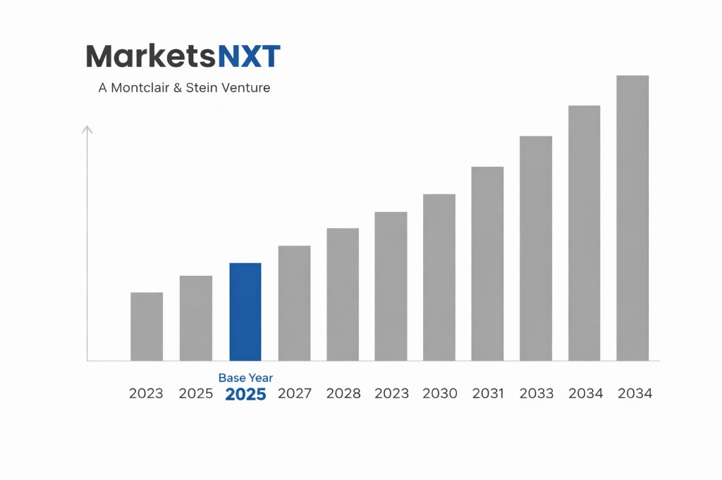
- ✓Base Year: 2025
- ✓Forecast Period: 2026–2034
Our Analytical Position on This Market
We believe silicon carbide power semiconductors are the most commercially underappreciated enabling technology of the energy transition — EV traction inverters, solar PV inverters, and bidirectional EV chargers all depend on SiC switching performance that silicon cannot achieve, creating structural supply constraints that will persist through 2027–2028 despite aggressive capacity expansion.
Industry Snapshot
The Power Electronics (SiC and GaN) market was valued at approximately USD 5.8 billion in 2024 and is projected to reach approximately USD 28.6 billion by 2034, growing at a CAGR of 17.3%–19.1%. Silicon carbide (SiC) and gallium nitride (GaN) wide-bandgap semiconductors enable power conversion at higher voltage, higher temperature, and lower switching loss than silicon — making them essential for high-efficiency EV traction inverters, solar and wind inverters, industrial motor drives, and fast-charging infrastructure that the energy transition requires at commercial scale.
What Is Structurally Pulling This Market Forward
EV traction inverter adoption of SiC is the dominant demand driver — Tesla's Model 3 (2018) was the first mass-market EV to use SiC MOSFETs in the main traction inverter, demonstrating 5–8% range improvement and 20–30% reduction in inverter size versus silicon IGBT. Every major EV OEM has committed to SiC traction inverters for premium EV lines by 2026–2027 — BMW i Series, Volkswagen ID platform, Hyundai IONIQ 6, and Stellantis EV platforms are all designed around SiC. The SiC supply constraint — capacity is booked 2–3 years forward at leading suppliers — is a demand signal, not a weakness: it reflects genuine committed OEM procurement above production capacity. Solar and wind power electronics is the second largest demand driver — SiC and GaN inverters for solar PV and battery energy storage achieve 99%+ conversion efficiency versus 97%–98% for silicon, with the efficiency gain directly reducing LCOE for gigawatt-scale solar installations.
The Friction Points That Matter
SiC wafer substrate supply is the primary structural constraint — SiC single-crystal growth (Lely method or sublimation) is extraordinarily slow (1–3mm per hour versus 1–2mm per minute for silicon), and SiC wafer yield (percentage of wafers without fatal crystal defects) is 50%–70% versus 95%+ for silicon. Wolfspeed controls approximately 60%–65% of the global SiC substrate market and has repeatedly guided supply as the bottleneck constraining SiC device manufacturer output. Its Mohawk Valley 200mm SiC wafer facility (Marcy, New York — the world's first 200mm SiC fab, supported by USD 2.5 billion DOE loan guarantee) and John Palmour Manufacturing Center (Durham, North Carolina) represent the most significant SiC substrate capacity expansions globally, but full volume ramp takes 3–5 years from groundbreaking.
Where Consensus Is Right, Wrong, and Missing the Point
Consensus is right that SiC will achieve 80%+ penetration of EV traction inverters in premium EVs above USD 40,000 by 2027 — OEM design commitments make this projection credible. Consensus is wrong about GaN adoption in automotive — most forecasts project rapid GaN adoption in EV onboard chargers and 400V/800V bidirectional charging by 2026, but GaN reliability qualification for automotive (AEC-Q101) by GaN power device manufacturers is proceeding more slowly than optimistic forecasts assumed, with Toyota and General Motors delaying some GaN OBC implementations to 2027–2028. What to watch: Wolfspeed Mohawk Valley 200mm wafer yield trajectory (quarterly conference call data point); Infineon SiC CoolSiC MOSFET automotive qualification status; and CREE's rebrand implementation and investor day guidance on 200mm wafer capacity economics.
The Opportunities This Market Will Reward
Near-term opportunity is SiC module manufacturing for bidirectional EV charging — vehicle-to-grid (V2G) chargers require power electronics that manage bidirectional power flow at 11–22 kW with high efficiency and compact form factor, a specification that SiC enables but silicon IGBTs cannot achieve at competitive cost and size. The V2G charger market is estimated at USD 2–4 billion by 2028, growing at 40%+ as utility companies and EV manufacturers develop V2G programmes. Mid-term opportunity is GaN for data centre power conversion — GaN transistors operating at MHz switching frequencies versus silicon's 50–200 kHz enable smaller, lighter power supply units for AI server racks that require 50–100 kW per rack at 95%+ efficiency. Meta, Google, and Microsoft are all developing GaN power supply specifications for next-generation AI data centre racks, representing a USD 3–5 billion GaN PSU market by 2030.
Market at a Glance
| Parameter | Details |
|---|---|
| Market Size 2025 | Approximately USD 6.8 billion |
| Market Size 2034 | Approximately USD 28.6 billion |
| Market Growth Rate | 17.3%–19.1% |
| Thesis Direction | Accelerating — SiC supply-constrained; GaN entering data centre |
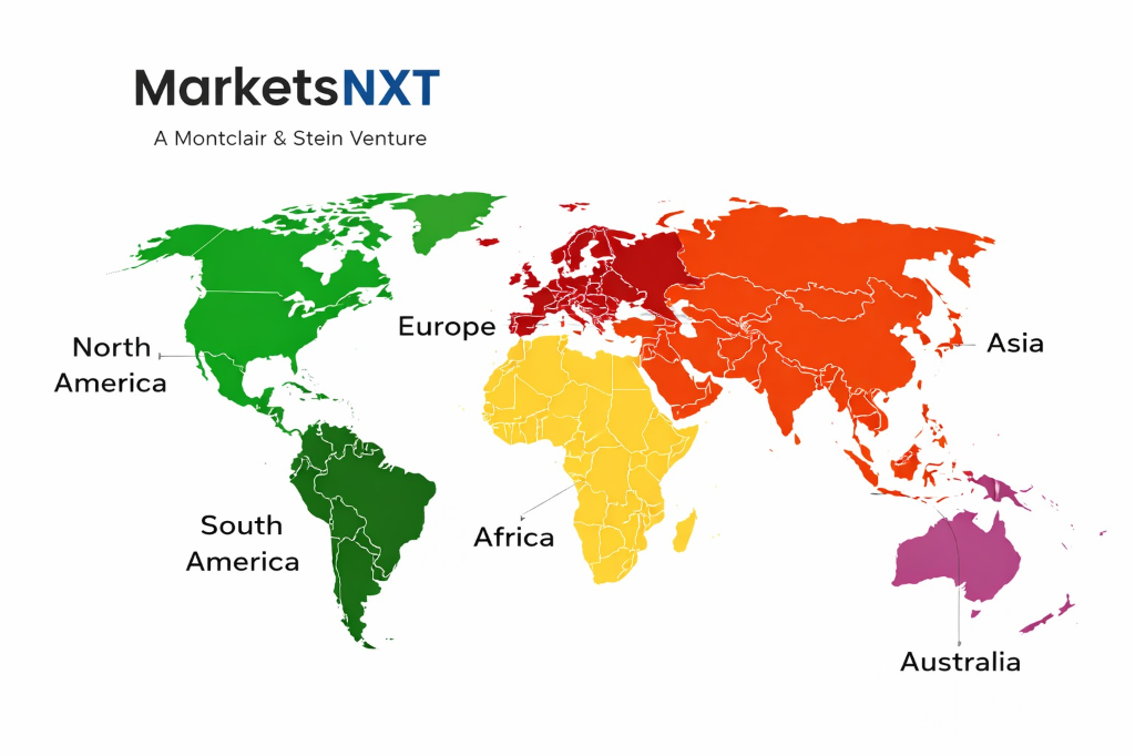
| Largest Region | Asia Pacific (Japan — Rohm, Mitsubishi Electric; China — Sanan, CREE China; Taiwan — GlobalWafers) |
| Segments Covered | SiC Power MOSFETs and Diodes, GaN HEMTs and Power ICs, SiC Substrates and Epitaxial Wafers, Power Modules (Traction Inverters) |
Regional Breakdown: Where Growth Is Coming From
Asia Pacific accounts for approximately 45%–50% of SiC and GaN power device manufacturing, with Japan (Rohm Semiconductor, Mitsubishi Electric), China (CREE China expansion, Sanan Optoelectronics), and Taiwan (UMC GaN, GlobalWafers SiC substrates) as the primary production centres. China's domestic SiC industry — SICC Technology, TankeBlue Semiconductor, Sanan Optoelectronics — is growing at 50%+ annually from a small base, targeting domestic EV supply chain requirements under Semiconductor Self-Reliance strategy. Europe accounts for approximately 25%–28%, dominated by STMicroelectronics (SiC devices) and Infineon Technologies (SiC and GaN), both with major SiC wafer processing facilities in Italy and Germany.
The Competitive Dynamics Shaping Market Share
The SiC competitive structure is vertically integrated at the substrate level — Wolfspeed supplies substrates to Onsemi, Renesas, and Infineon who use them for device manufacturing, while simultaneously competing with device manufacturing under its own brand. STMicroelectronics is the most advanced vertically integrated SiC manufacturer outside Wolfspeed, operating its own SiC epitaxial wafer processing from third-party substrate. Infineon's SiC CoolSiC MOSFET is the strongest automotive design-in competitor to Onsemi's 2nd generation EliteSiC and STMicro's SiC devices. Chinese domestic SiC manufacturers are closing the quality gap — Sanan's SiC MOSFET samples are being qualified by Chinese EV OEMs including BYD and XPENG — creating a parallel domestic supply chain that reduces Chinese EV dependence on Western SiC suppliers.
Leading Market Participants
- Wolfspeed
- STMicroelectronics
- Onsemi
- Infineon Technologies
- Rohm Semiconductor
- SUEZ
- Veolia
- Siemens Energy
- Eaton
- ABB
Long-Term Market Perspective
By 2034, SiC will be the dominant power semiconductor for EV traction inverters above 200kW, industrial motor drives above 100kW, and solar/wind inverters above 50kW — with silicon remaining in lower-voltage and lower-efficiency applications. GaN will be established in data centre power supplies, consumer fast chargers, and EV onboard chargers where its MHz switching frequency advantage enables the smallest power conversion form factors. The 200mm SiC wafer transition — adding 50% more chips per wafer versus current 150mm production — will be the key supply cost reduction event enabling SiC to reach silicon IGBT price parity for 400V automotive applications by 2027–2029.
Frequently Asked Questions
Market Segmentation
- SiC MOSFETs and Schottky Diodes (Automotive and Industrial)
- GaN HEMTs and Power ICs (Consumer and Data Centre)
- SiC Bare Wafers and Epitaxial Substrates
- Others (SiC Power Modules, GaN RF Devices, Diamond Semiconductors)
- Electric Vehicle Traction Inverters and OBC
- Solar and Wind Power Inverters
- Industrial Motor Drives and Variable Speed Drives
- Data Centre Power Supplies and UPS
- Fast Charging Infrastructure (AC and DC)
- Direct OEM Design-In (Automotive Tier 1 and EV OEM)
- Distribution (Arrow, Avnet, Mouser)
- Government Strategic Reserve and Defence Contracts
- Joint Development Agreement and Foundry Services
- North America
- Europe
- Asia Pacific
- Latin America
- Middle East and Africa
Table of Contents
Research Framework and Methodological Approach
Information
Procurement
Information
Analysis
Market Formulation
& Validation
Overview of Our Research Process
MarketsNXT follows a structured, multi-stage research framework designed to ensure accuracy, reliability, and strategic relevance of every published study. Our methodology integrates globally accepted research standards with industry best practices in data collection, modeling, verification, and insight generation.
1. Data Acquisition Strategy
Robust data collection is the foundation of our analytical process. MarketsNXT employs a layered sourcing model.
- Company annual reports & SEC filings
- Industry association publications
- Technical journals & white papers
- Government databases (World Bank, OECD)
- Paid commercial databases
- KOL Interviews (CEOs, Marketing Heads)
- Surveys with industry participants
- Distributor & supplier discussions
- End-user feedback loops
- Questionnaires for gap analysis
Analytical Modeling and Insight Development
After collection, datasets are processed and interpreted using multiple analytical techniques to identify baseline market values, demand patterns, growth drivers, constraints, and opportunity clusters.
2. Market Estimation Techniques
MarketsNXT applies multiple estimation pathways to strengthen forecast accuracy.
Bottom-up Approach
Aggregating granular demand data from country level to derive global figures.
Top-down Approach
Breaking down the parent industry market to identify the target serviceable market.
Supply Chain Anchored Forecasting
MarketsNXT integrates value chain intelligence into its forecasting structure to ensure commercial realism and operational alignment.
Supply-Side Evaluation
Revenue and capacity estimates are developed through company financial reviews, product portfolio mapping, benchmarking of competitive positioning, and commercialization tracking.
3. Market Engineering & Validation
Market engineering involves the triangulation of data from multiple sources to minimize errors.
Extensive gathering of raw data.
Statistical regression & trend analysis.
Cross-verification with experts.
Publication of market study.
Client-Centric Research Delivery
MarketsNXT positions research delivery as a collaborative engagement rather than a static information transfer. Analysts work with clients to clarify objectives, interpret findings, and connect insights to strategic decisions.