Semiconductor Manufacturing Equipment Market Size, Share & Forecast 2026–2034
Report Highlights
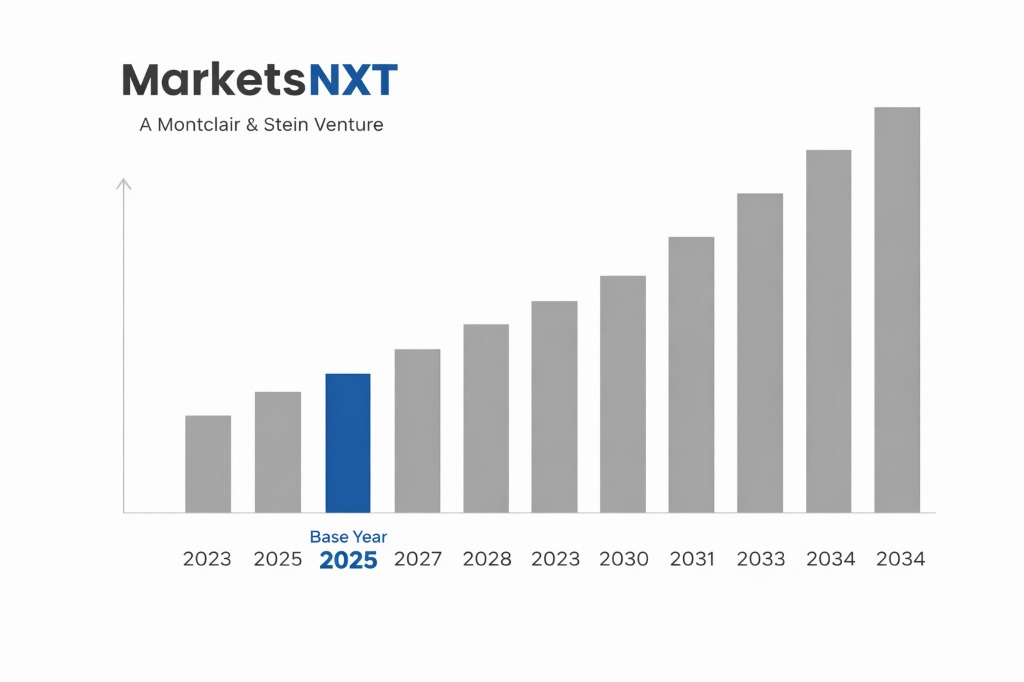
- ✓Market Size 2024: $118.7 billion
- ✓Market Size 2034: $267.4 billion
- ✓CAGR: 8.4%
- ✓Market Definition: Equipment used to manufacture semiconductor devices including wafer fabrication, assembly, test, and packaging systems. Encompasses lithography, etching, deposition, inspection, and metrology tools across front-end and back-end processes.
- ✓Leading Companies: ASML, Applied Materials, Tokyo Electron, KLA Corporation, Lam Research
- ✓Base Year: 2025
- ✓Forecast Period: 2026–2034
How the Semiconductor Manufacturing Equipment Market Works: Supply Chain Explained
The semiconductor manufacturing equipment supply chain begins with specialized materials including ultra-pure silicon wafers from Japan and Taiwan, photoresists and specialty chemicals from companies in Germany and Japan, and precision optical components manufactured primarily in Germany and the Netherlands. Advanced lithography systems require extreme ultraviolet light sources, mirrors with near-perfect reflectivity, and photomasks produced in dedicated facilities. Key processing steps include wafer preparation, photolithography, etching, ion implantation, chemical vapor deposition, and metrology, with each requiring specialized equipment manufactured by different suppliers across the United States, Japan, Netherlands, and South Korea. Critical subsystems like vacuum chambers, precision robotics, and control software integrate components from hundreds of suppliers globally.
Finished semiconductor manufacturing equipment reaches customers through direct sales relationships with semiconductor foundries and integrated device manufacturers, typically involving 12-24 month lead times for complex systems. Equipment pricing follows cost-plus models with significant customization premiums, while service contracts generate recurring revenue streams representing 20-30% of total equipment value over system lifetime. Distribution occurs through regional service centers providing installation, training, and maintenance support, with spare parts inventory strategically positioned near major semiconductor manufacturing hubs in Taiwan, South Korea, China, and the United States. Value concentration occurs at the system integration level, where equipment manufacturers capture 40-60% of total supply chain margin through proprietary process technologies and specialized engineering capabilities.
Semiconductor Manufacturing Equipment Market Dynamics
The semiconductor equipment market operates on cyclical demand patterns driven by foundry capital expenditure cycles and technology node transitions, with pricing power concentrated among suppliers of critical process tools like extreme ultraviolet lithography systems and advanced etching equipment. Contract structures typically involve multi-year agreements with staged payments linked to equipment delivery milestones, acceptance testing, and performance guarantees, while buyers maintain qualified vendor lists limiting supplier options for critical processes. Market transactions reflect high switching costs due to process integration requirements and intellectual property dependencies, creating customer stickiness that allows equipment suppliers to maintain pricing leverage during demand upturns.
Information asymmetries exist around process yield optimization and equipment reliability data, with suppliers leveraging proprietary process knowledge to differentiate their offerings and justify premium pricing. The market exhibits oligopolistic characteristics in advanced technology segments, where 2-3 suppliers control 70-90% market share for specific process steps, while commodity segments like older-generation tools face intense price competition. Buyer-seller relationships involve deep technical collaboration throughout equipment development cycles, with foundries providing process requirements and feedback that influence next-generation equipment specifications and roadmaps.
Growth Drivers Fuelling Semiconductor Manufacturing Equipment Expansion
Artificial intelligence and high-performance computing demand drives increased investment in advanced packaging equipment and specialized test systems, requiring suppliers to expand production capacity for wire bonding systems, flip-chip packaging tools, and high-frequency test equipment. This translates into heightened demand for precision dispensing systems, advanced thermal management solutions, and multi-site parallel testing capabilities that reduce per-unit test costs while maintaining quality standards. Memory manufacturers require specialized equipment for 3D NAND and next-generation DRAM architectures, increasing orders for atomic layer deposition systems, plasma etching tools, and metrology equipment capable of measuring features at sub-10 nanometer dimensions.
Automotive electrification and 5G infrastructure deployment necessitate expanded production of power semiconductors and RF components, driving investment in silicon carbide and gallium nitride processing equipment including high-temperature furnaces, ion implantation systems, and specialized metallization tools. Edge computing proliferation increases demand for specialized packaging equipment supporting system-in-package architectures, requiring suppliers to develop advanced die bonding, encapsulation, and testing systems. Geopolitical supply chain diversification efforts stimulate new fab construction in North America and Europe, creating demand for complete equipment sets spanning wafer fabrication through final test and assembly operations.
Supply Chain Risks and Market Restraints
Geographic concentration of critical suppliers creates significant vulnerabilities, with ASML maintaining monopoly position in extreme ultraviolet lithography systems manufactured exclusively in the Netherlands, while specialized optical components and photomasks depend heavily on Japanese suppliers including Shin-Etsu Chemical and Hoya Corporation. Single-source dependencies exist for advanced process chemicals and rare earth materials used in ion implantation equipment, with China controlling 80% of rare earth oxide production required for equipment manufacturing. Supply chain disruptions affect precision mechanical components sourced from specialized manufacturers in Germany and Switzerland, where lead times extend 40-52 weeks for complex vacuum systems and robotics assemblies.
Regulatory trade restrictions limit technology transfer and equipment sales to specific countries, affecting revenue streams and forcing suppliers to maintain separate product lines and manufacturing facilities for different geographic markets. Environmental regulations increasingly constrain perfluorinated compound usage in semiconductor processing, requiring equipment redesign and alternative chemistry development that delays new product introductions. Skilled technician shortages affect equipment installation and maintenance capabilities, with suppliers struggling to maintain adequate field service coverage as semiconductor manufacturing capacity expands globally, particularly in emerging fabrication regions lacking established technical infrastructure and trained personnel.
Where Semiconductor Manufacturing Equipment Growth Opportunities Are Emerging
Advanced packaging technology transitions create opportunities for suppliers developing hybrid bonding systems, through-silicon-via processing equipment, and fan-out wafer-level packaging tools, with assembly equipment manufacturers capturing higher margins through proprietary process integration capabilities. Emerging compound semiconductor applications including silicon carbide power devices and gallium arsenide RF components require specialized high-temperature processing equipment and ion implantation systems, enabling suppliers to command premium pricing for customized solutions. Chiplet architecture adoption drives demand for advanced die-to-die interconnect processing equipment and multi-chip module assembly systems, where equipment suppliers can differentiate through yield optimization and throughput capabilities.
Artificial intelligence chip manufacturing requires specialized equipment for advanced memory architectures including processing-in-memory devices and neuromorphic computing components, creating opportunities for suppliers developing novel deposition and patterning technologies. Carbon nanotube and graphene-based semiconductor devices represent emerging applications requiring entirely new equipment categories for material synthesis and device fabrication, where early-moving suppliers can establish dominant positions. Manufacturing localization initiatives in India, Southeast Asia, and Latin America create demand for complete equipment ecosystems including refurbished and previous-generation systems, enabling suppliers to monetize older technology platforms while supporting emerging market semiconductor production capabilities.
Market at a Glance
| Metric | Value |
|---|---|
| Market Size 2024 | $118.7 billion |
| Market Size 2034 | $267.4 billion |
| Growth Rate (CAGR) | 8.4% |
| Most Critical Decision Factor | Process technology capability and yield optimization |
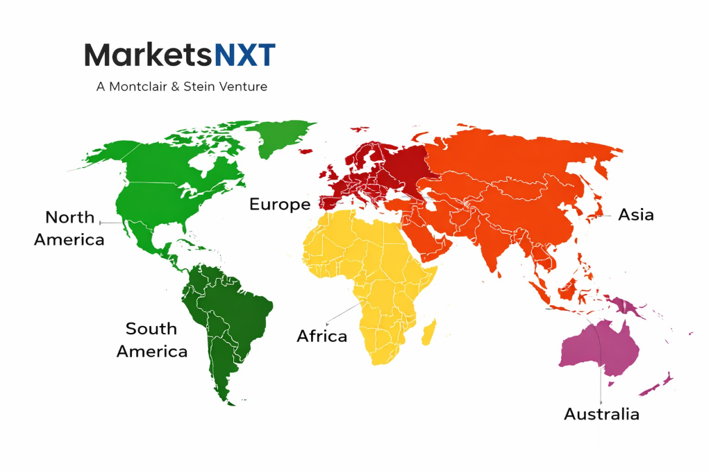
| Largest Region | Asia Pacific |
| Competitive Structure | Oligopolistic with specialized niches |
Regional Supply and Demand Map
Asia Pacific dominates semiconductor equipment production and consumption, with Taiwan, South Korea, and China accounting for 65% of global equipment installations driven by foundry expansion and memory manufacturing capacity additions. Japan maintains critical supply positions in materials and precision components, while South Korean companies like Samsung and SK Hynix drive significant equipment demand through memory technology transitions. The Netherlands supplies advanced lithography systems exclusively through ASML, while the United States concentrates equipment design and high-end manufacturing through Applied Materials, Lam Research, and KLA Corporation, with production facilities spanning California, Oregon, and Massachusetts.
Europe serves as a key supplier of specialty materials and precision mechanical components, with Germany providing advanced robotics and vacuum systems while supplying critical chemicals through companies like Merck KGaA. North American demand centers on logic device manufacturing and advanced packaging operations, while Latin American markets remain limited to assembly and test equipment requirements. Trade flows reflect technology export controls, with advanced equipment restricted to trusted countries, creating parallel supply chains for different technology generations and customer segments across established and emerging semiconductor manufacturing regions.
Leading Market Participants
- ASML Holding
- Applied Materials
- Tokyo Electron
- KLA Corporation
- Lam Research
- SCREEN Semiconductor Solutions
- Teradyne
- Advantest
- ASM International
- Kulicke and Soffa
Long-Term Semiconductor Manufacturing Equipment Outlook
By 2034, the semiconductor equipment supply chain will undergo substantial reconfiguration driven by geopolitical considerations and technology localization requirements, with parallel equipment ecosystems emerging to serve different regional markets and technology access levels. Advanced packaging and heterogeneous integration will dominate equipment demand growth, requiring suppliers to develop integrated process flows spanning traditional wafer fabrication and assembly operations. Artificial intelligence optimization of manufacturing processes will transform equipment design and operation, with predictive maintenance and autonomous process control becoming standard features across all equipment categories.
The most valuable supply chain positions in 2034 will be advanced lithography systems for sub-3 nanometer processes, specialized packaging equipment for chiplet integration, and AI-optimized metrology systems providing real-time process feedback and control. Current market leaders ASML, Applied Materials, and Tokyo Electron appear best positioned to capture this value through continued R&D investment and customer partnership strategies, while emerging opportunities in quantum computing and photonic device manufacturing may enable new entrants to establish dominant positions in nascent technology segments requiring entirely novel equipment approaches and capabilities.
Frequently Asked Questions
Market Segmentation
- Wafer Processing Equipment
- Assembly and Packaging Equipment
- Test Equipment
- Other Equipment
- Below 10nm
- 10nm-22nm
- 23nm-45nm
- Above 45nm
- Foundries
- Memory Manufacturers
- IDMs
- Others
- Logic
- Memory
- Analog
- Discrete
Table of Contents
1.1 Research Methodology / 1.2 Scope and Definitions / 1.3 Data Sources
Chapter 02 Executive Summary
2.1 Report Highlights / 2.2 Market Size and Forecast 2024-2034
Chapter 03 Semiconductor Manufacturing Equipment - Industry Analysis
3.1 Market Overview / 3.2 Market Dynamics / 3.3 Growth Drivers
3.4 Restraints / 3.5 Opportunities
Chapter 04 Equipment Type Insights
Chapter 05 Technology Node Insights
Chapter 06 End User Insights
Chapter 07 Application Insights
Chapter 08 Semiconductor Manufacturing Equipment - Regional Insights
8.1 North America / 8.2 Europe / 8.3 Asia Pacific
8.4 Latin America / 8.5 Middle East and Africa
Chapter 09 Competitive Landscape
9.1 Competitive Overview / 9.2 Market Share Analysis
9.3 Leading Market Participants
9.3.1 ASML Holding / 9.3.2 Applied Materials / 9.3.3 Tokyo Electron
9.3.4 KLA Corporation / 9.3.5 Lam Research / 9.3.6 SCREEN Semiconductor Solutions
9.3.7 Teradyne / 9.3.8 Advantest / 9.3.9 ASM International / 9.3.10 Kulicke and Soffa
9.4 Outlook
Research Framework and Methodological Approach
Information
Procurement
Information
Analysis
Market Formulation
& Validation
Overview of Our Research Process
MarketsNXT follows a structured, multi-stage research framework designed to ensure accuracy, reliability, and strategic relevance of every published study. Our methodology integrates globally accepted research standards with industry best practices in data collection, modeling, verification, and insight generation.
1. Data Acquisition Strategy
Robust data collection is the foundation of our analytical process. MarketsNXT employs a layered sourcing model.
- Company annual reports & SEC filings
- Industry association publications
- Technical journals & white papers
- Government databases (World Bank, OECD)
- Paid commercial databases
- KOL Interviews (CEOs, Marketing Heads)
- Surveys with industry participants
- Distributor & supplier discussions
- End-user feedback loops
- Questionnaires for gap analysis
Analytical Modeling and Insight Development
After collection, datasets are processed and interpreted using multiple analytical techniques to identify baseline market values, demand patterns, growth drivers, constraints, and opportunity clusters.
2. Market Estimation Techniques
MarketsNXT applies multiple estimation pathways to strengthen forecast accuracy.
Bottom-up Approach
Aggregating granular demand data from country level to derive global figures.
Top-down Approach
Breaking down the parent industry market to identify the target serviceable market.
Supply Chain Anchored Forecasting
MarketsNXT integrates value chain intelligence into its forecasting structure to ensure commercial realism and operational alignment.
Supply-Side Evaluation
Revenue and capacity estimates are developed through company financial reviews, product portfolio mapping, benchmarking of competitive positioning, and commercialization tracking.
3. Market Engineering & Validation
Market engineering involves the triangulation of data from multiple sources to minimize errors.
Extensive gathering of raw data.
Statistical regression & trend analysis.
Cross-verification with experts.
Publication of market study.
Client-Centric Research Delivery
MarketsNXT positions research delivery as a collaborative engagement rather than a static information transfer. Analysts work with clients to clarify objectives, interpret findings, and connect insights to strategic decisions.