Acoustic Microscope Market (Scanning Acoustic Microscopy, C-SAM, Through-Transmission, Pulse-Echo, Semiconductor Packaging, Electronics, Medical Devices, Aerospace, Automotive, Failure Analysis, Quality Control) – Global Market Size, Share, Growth, Trends, Statistics Analysis Report, By Region, and Forecast 2026–2034
Market Overview
Report Highlights
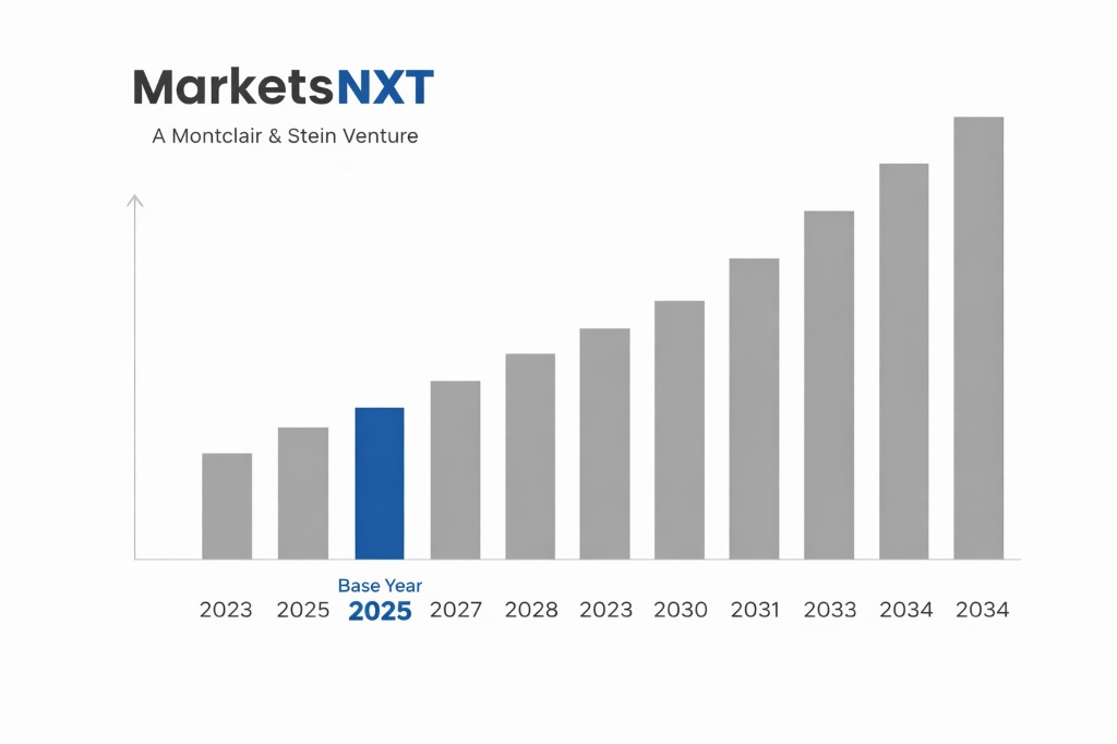
. The Acoustic Microscope market was valued at approximately USD 312 million in 2024 and is projected to reach approximately USD 698 million by 2034.
. The market is growing at a CAGR of 8.4% from 2025 to 2034.
. Acoustic Microscopes are non-destructive testing instruments that use focused ultrasound waves to image internal structures, detect delaminations, voids, cracks, and bonding defects within solid materials and electronic components without requiring physical sectioning or destruction of the sample.
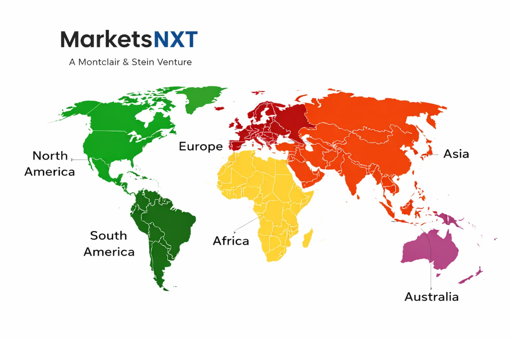
. North America holds the largest regional share at approximately 37% in 2024.
. Asia Pacific is the fastest-growing region, driven by semiconductor packaging quality inspection demand from advanced packaging facilities in Taiwan, South Korea, China, and Japan.
. Key segments covered: Technology (C-SAM, Through-Transmission, Pulse-Echo), Application (Semiconductor Packaging, Electronics, Medical Devices, Aerospace, Automotive), Use Case (Failure Analysis, Quality Control).
. Key players: Sonoscan, PVA TePla, Hitachi Power Solutions, Nikon, Nordson DAGE, Kraemer Sonic Industries, SEC, Sonix, Insight K.K., Olympus.
. Strategic insights: advanced semiconductor packaging inspection, electric vehicle component quality control, and medical implant integrity verification are the primary growth levers.
. Base year: 2025. Forecast period: 2026–2034.
. Regions covered: North America, Europe, Asia Pacific, Latin America, Middle East & Africa.
Industry Snapshot
The Acoustic Microscope market was valued at approximately USD 312 million in 2024 and is expected to reach approximately USD 698 million by 2034, growing at a CAGR of 8.4% from 2025 to 2034. Acoustic microscopy occupies a unique and indispensable niche in the non-destructive testing and inspection landscape, providing the ability to image internal features of solid samples using focused ultrasound without the ionizing radiation concerns of X-ray techniques and without the destructive sample preparation required for cross-sectional optical or electron microscopy. The technology is particularly critical in semiconductor packaging quality control, where the reliability of advanced chip packages depends on void-free die attach materials, intact wire bond and flip-chip connections, and defect-free encapsulant coverage that only acoustic microscopy can verify non-destructively with sufficient resolution and throughput for production environments. The market is being driven by the escalating complexity and reliability requirements of advanced semiconductor packaging, the expansion of quality-critical electronics in automotive and medical applications, and the growing adoption of acoustic microscopy beyond traditional failure analysis into inline production quality control applications.
Key Market Growth Catalysts
Advanced semiconductor packaging technology proliferation is the most powerful growth driver for acoustic microscopy, as chiplet integration, 3D IC stacking, flip-chip BGA packages, and power device modules all create complex internal interfaces and bonding layers where void formation, delamination, and incomplete bonding must be detected before field deployment. Automotive electronics reliability requirements are intensifying inspection investment as the safety-critical nature of ADAS sensors, power modules, and battery management electronics in electric vehicles demands thorough quality verification at levels that traditional surface inspection cannot provide. Medical device quality assurance requirements for implantable and life-critical electronics, including pacemaker hermetic packaging, cochlear implant electronics, and neurostimulator assemblies, create a high-value application segment where acoustic microscopy provides the non-destructive internal imaging capability that regulatory compliance and reliability standards require. Government semiconductor manufacturing investment programs funding new advanced packaging facilities are creating substantial procurement demand for inspection equipment including acoustic microscopes.
Market Challenges and Constraints
Acoustic microscopy faces application limitations arising from the requirement for liquid coupling between the ultrasonic transducer and the sample surface, which complicates inspection of moisture-sensitive components and limits the technology's applicability for some semiconductor packages that cannot tolerate water immersion even briefly during inspection. Throughput constraints relative to X-ray inspection for certain defect types limit acoustic microscopy's competitiveness for high-volume production screening applications where X-ray systems can inspect more samples per hour with acceptable defect detection capability for specific defect categories. The requirement for skilled operators capable of interpreting acoustic microscopy images and distinguishing genuine defects from imaging artifacts requires trained personnel investment that represents an operational overhead for laboratories adding acoustic inspection capability. The relatively small size of the acoustic microscope market compared to semiconductor process control equipment categories limits the R&D investment available for technology advancement and the commercial viability of multiple competing platform approaches.
Strategic Growth Opportunities
Automated inline acoustic inspection integration into semiconductor packaging production lines represents a significant market expansion opportunity, transforming acoustic microscopy from primarily a laboratory failure analysis and sampling inspection tool into a production-rate quality gate that inspects every package before shipment. Electric vehicle power electronics inspection represents a high-growth application, as IGBT and silicon carbide power modules used in EV inverters and onboard chargers require acoustic inspection of solder and silver sinter die attach layers where voiding above defined limits degrades thermal management performance and long-term reliability. Advanced packaging technologies including hybrid bonding, through-silicon via verification, and wafer-level fan-out packaging are creating new acoustic microscopy application requirements that drive demand for higher-frequency transducers and improved image resolution capability in next-generation systems. Additive manufacturing quality verification is an emerging application where acoustic microscopy can provide non-destructive internal porosity and delamination imaging that supports quality assurance for 3D-printed metal and polymer components in aerospace and medical device applications.
Market Coverage Overview
Parameter | Details
Market Size in 2025 | USD 338 million
Market Size in 2034 | USD 698 million
Market Growth Rate (2026–2034) | CAGR of 8.4%
Largest Market | North America
Segments Covered | Technology, Application, Use Case
Regions Covered | North America, Europe, Asia Pacific, Latin America, Middle East & Africa
Geographic Performance Analysis
North America leads the Acoustic Microscope market, driven by the United States' concentration of semiconductor failure analysis laboratories, advanced electronics manufacturing quality programs, medical device manufacturing requiring rigorous non-destructive testing, and aerospace and defense electronics inspection requirements. Sonoscan, the market's leading vendor, is headquartered in the United States, reflecting the country's long-standing leadership in acoustic microscopy technology development. Asia Pacific is the fastest-growing region, with Taiwan's OSAT and advanced packaging industry, South Korea's semiconductor and display manufacturing, Japan's precision electronics quality culture, and China's expanding semiconductor packaging sector collectively generating the largest volume of acoustic microscopy equipment demand. Europe maintains a significant market through automotive electronics manufacturing in Germany and medical device production across Germany, Switzerland, and Ireland, both of which are major acoustic microscopy users. Latin America and Middle East and Africa are smaller markets with demand concentrated in electronics manufacturing and research institution applications.
Competitive Environment Analysis
The Acoustic Microscope market is small and relatively concentrated, with Sonoscan maintaining a leading position in the semiconductor and electronics market through its C-SAM technology platform and established customer base among major semiconductor manufacturers and contract assembly houses globally. PVA TePla, Hitachi Power Solutions, and Nordson DAGE compete in the semiconductor packaging inspection segment with their respective platform offerings. Nikon and Olympus bring broader precision imaging brand equity to the acoustic microscopy market. Competition centers on image resolution and frequency range capability for advanced packaging inspection, system throughput for production quality control applications, software analysis capability for automated defect classification, and application support expertise for specific customer inspection challenges. Market size constraints limit the number of viable commercial competitors to a small field, making technology leadership and application expertise the primary competitive differentiators.
Leading Market Participants
Sonoscan
PVA TePla
Hitachi Power Solutions
Nikon
Nordson DAGE
Kraemer Sonic Industries
SEC (Scanning Electron Microscope & Equipment)
Sonix
Insight K.K.
Olympus
Long-Term Market Perspective
The Acoustic Microscope market's long-term growth is anchored in the escalating internal structure complexity and reliability requirements of advanced semiconductor packaging, automotive power electronics, and medical device manufacturing that create persistent and growing demand for non-destructive internal imaging capability. Advanced packaging technology advancement, including higher-density chiplet integration, tighter thermal performance requirements, and more complex bonding interfaces, will progressively increase the criticality and resolution requirements of acoustic inspection in semiconductor quality management. Electric vehicle adoption will sustain long-term demand growth from power electronics quality programs as the scale of EV production increases and as reliability data from field deployments reinforces the importance of thorough factory inspection in preventing field failures. Automation of acoustic microscopy through robotic sample handling, AI-powered defect classification, and inline process integration will expand the technology's addressable market from laboratory inspection toward production-rate quality control, substantially increasing per-facility instrument utilization and total market scale.
Market Segmentation
- C-SAM (Scanning Acoustic Microscopy)
- Through-Transmission
- Pulse-Echo
- Others
- Semiconductor Packaging
- Electronics Manufacturing
- Medical Devices
- Aerospace
- Automotive
- Others
- Failure Analysis
- Quality Control
- Others
Frequently Asked Questions
Market Segmentation
- C-SAM (Scanning Acoustic Microscopy)
- Through-Transmission
- Pulse-Echo
- Others
- Semiconductor Packaging
- Electronics Manufacturing
- Medical Devices
- Aerospace
- Automotive
- Others
- Failure Analysis
- Quality Control
- Others
Table of Contents
Chapter 01 Methodology & Scope
1.1 Data Analysis Models
1.2 Research Scope & Assumptions
1.3 List of Data Sources
Chapter 02 Executive Summary
2.1 Market Overview
2.2 Acoustic Microscope Market Size, 2023 to 2034
2.2.1 Market Analysis, 2023 to 2034
2.2.2 Market Analysis, by Region, 2023 to 2034
2.2.3 Market Analysis, by Technology, 2023 to 2034
2.2.4 Market Analysis, by Application, 2023 to 2034
2.2.5 Market Analysis, by Use Case, 2023 to 2034
Chapter 03 Acoustic Microscope Market – Industry Analysis
3.1 Market Segmentation
3.2 Market Definitions and Assumptions
3.3 Porter's Five Force Analysis
3.4 PEST Analysis
3.5 Market Dynamics
3.5.1 Market Driver Analysis
3.5.2 Market Restraint Analysis
3.5.3 Market Opportunity Analysis
3.6 Value Chain and Industry Mapping
3.7 Regulatory and Standards Landscape
Chapter 04 Acoustic Microscope Market – Technology Insights
4.2 Through-Transmission
4.3 Pulse-Echo
4.4 Others
Chapter 05 Acoustic Microscope Market – Application Insights
5.1 Semiconductor Packaging
5.2 Electronics Manufacturing
5.3 Medical Devices
5.4 Aerospace
5.5 Automotive
5.6 Others
Chapter 06 Acoustic Microscope Market – Use Case Insights
6.1 Failure Analysis
6.2 Quality Control
6.3 Others
Chapter 07 Acoustic Microscope Market – Regional Insights
7.1 By Region Overview
7.2 North America
7.3 Europe
7.4 Asia Pacific
7.5 Latin America
7.6 Middle East & Africa
Chapter 08 Competitive Landscape
8.1 Competitive Heatmap
8.2 Market Share Analysis
8.3 Strategy Benchmarking
8.4 Company Profiles
Research Framework and Methodological Approach
Information
Procurement
Information
Analysis
Market Formulation
& Validation
Overview of Our Research Process
MarketsNXT follows a structured, multi-stage research framework designed to ensure accuracy, reliability, and strategic relevance of every published study. Our methodology integrates globally accepted research standards with industry best practices in data collection, modeling, verification, and insight generation.
1. Data Acquisition Strategy
Robust data collection is the foundation of our analytical process. MarketsNXT employs a layered sourcing model.
- Company annual reports & SEC filings
- Industry association publications
- Technical journals & white papers
- Government databases (World Bank, OECD)
- Paid commercial databases
- KOL Interviews (CEOs, Marketing Heads)
- Surveys with industry participants
- Distributor & supplier discussions
- End-user feedback loops
- Questionnaires for gap analysis
Analytical Modeling and Insight Development
After collection, datasets are processed and interpreted using multiple analytical techniques to identify baseline market values, demand patterns, growth drivers, constraints, and opportunity clusters.
2. Market Estimation Techniques
MarketsNXT applies multiple estimation pathways to strengthen forecast accuracy.
Bottom-up Approach
Aggregating granular demand data from country level to derive global figures.
Top-down Approach
Breaking down the parent industry market to identify the target serviceable market.
Supply Chain Anchored Forecasting
MarketsNXT integrates value chain intelligence into its forecasting structure to ensure commercial realism and operational alignment.
Supply-Side Evaluation
Revenue and capacity estimates are developed through company financial reviews, product portfolio mapping, benchmarking of competitive positioning, and commercialization tracking.
3. Market Engineering & Validation
Market engineering involves the triangulation of data from multiple sources to minimize errors.
Extensive gathering of raw data.
Statistical regression & trend analysis.
Cross-verification with experts.
Publication of market study.
Client-Centric Research Delivery
MarketsNXT positions research delivery as a collaborative engagement rather than a static information transfer. Analysts work with clients to clarify objectives, interpret findings, and connect insights to strategic decisions.