AI Chip (GPU/TPU) Market Size, Share & Forecast 2026–2034
Report Highlights
- ✓Market Size 2024: Approximately USD 68.4 billion
- ✓Market Size 2034: Approximately USD 424.6 billion
- ✓CAGR Range: 20.0%–24.4%
- ✓Market Definition: The AI chip market encompasses semiconductor devices purpose-built or architecturally optimised for artificial intelligence workloads — including graphics processing units (GPUs) used for AI training and inference, tensor processing units (TPUs) developed by Google, AI-specific neural processing units (NPUs) in consumer devices, and custom ASIC accelerators deployed in hyperscaler data centres and edge AI applications
- ✓Top 3 Competitive Dynamics: NVIDIA's CUDA software ecosystem creating a switching cost moat that is as or more durable than its hardware performance advantage — the decades of developer code, tooling, and model libraries built on CUDA create a platform lock-in that AMD, Intel, and custom silicon cannot dislodge without matching the software investment; hyperscaler custom AI silicon (Google TPU, Amazon Trainium/Inferentia, Microsoft Maia, Meta MTIA) representing the most significant structural threat to NVIDIA's data centre GPU dominance by internalising the most predictable inference workloads; the Huawei Ascend chip ecosystem demonstrating that China can develop competitive AI silicon domestically despite US export controls, with implications for global market bifurcation
- ✓First 5 Companies: NVIDIA (H100/H200/Blackwell GPU), AMD (MI300 series), Google (TPU v5), Amazon (Trainium2), Intel (Gaudi3)
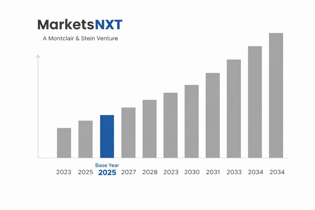
- ✓Base Year: 2025
- ✓Forecast Period: 2026–2034
- ✓Contrarian Insight: NVIDIA's AI chip dominance is more durable than critics of its valuation acknowledge — not because of hardware performance superiority (which AMD and custom silicon are narrowing) but because the CUDA ecosystem's developer inertia creates switching costs that are structural rather than technical; the realistic threat to NVIDIA's market position is not competitive GPU performance but hyperscaler workload migration from training to inference at scale, which favours custom silicon economics
Key Decisions This Report Supports
This report addresses four critical decisions facing technology executives, investors, and government policymakers in the AI chip market. The first is the procurement decision: whether to standardise on NVIDIA's GPU platform (maximum software compatibility, highest availability, premium pricing), diversify to AMD GPU or Intel Gaudi, or wait for hyperscaler custom silicon access through cloud API rather than data centre hardware procurement. The analysis framework: training workloads strongly favour NVIDIA CUDA ecosystem for performance and tooling compatibility; inference workloads have more viable alternatives where throughput-per-dollar is the primary metric. The second is the supply chain decision: given the Taiwan Semiconductor Manufacturing Company concentration of leading-edge AI chip production, how should companies assess geopolitical supply disruption risk and what hedging strategies are available? The third is the investment decision: at current valuation multiples, is NVIDIA's market position durable enough to justify continued premium versus AMD, Arm Holdings, and AI chip pure-plays? The fourth is the policy decision: how should governments evaluate AI chip export controls, domestic manufacturing incentives, and national AI computing infrastructure investments to preserve competitive advantage?
Industry Snapshot
The AI Chip (GPU/TPU) market was valued at approximately USD 68.4 billion in 2024 and is projected to reach approximately USD 424.6 billion by 2034, growing at a CAGR of 20.0%–24.4%. NVIDIA's data centre GPU segment alone generated approximately USD 47.5 billion in 2024 revenue — representing approximately 69% of the addressable market defined here. AMD's data centre GPU revenue (MI300X and MI300A) reached approximately USD 5 billion in 2024, growing from near-zero in 2022, demonstrating the fastest revenue ramp in semiconductor history for a new product family. Google's TPU v5 powers the majority of Google's own AI inference workloads and is available through Google Cloud, representing one of the most deployed but commercially reported AI accelerators. The market is growing at its fastest rate in semiconductor history — AI workload demand is growing faster than Moore's Law can supply performance improvement, driving unprecedented data centre capital expenditure from all major cloud providers.
The Forces Accelerating Demand Right Now
Generative AI model training and inference is the primary demand driver — and the demand is structurally expanding, not merely a cyclical wave. Each generation of frontier AI model requires approximately 10x the compute of its predecessor: GPT-3 required approximately 3×10²³ FLOPS; GPT-4 approximately 2×10²⁴ FLOPS; the models in development for 2026–2027 training runs are estimated at 10²⁵–10²⁶ FLOPS. This exponential scaling creates a sustained capital expenditure obligation for frontier AI companies and hyperscalers that is independent of current AI monetisation — Meta, Google, Microsoft, and Amazon each committed to USD 40–60 billion in 2024 AI infrastructure capital expenditure, with guidance for continued acceleration through 2026. The inference demand from deployed AI services — Google Search AI Overviews, Microsoft Copilot, ChatGPT, Claude — is growing at 15%–25% monthly as user adoption expands and use case complexity increases, creating a recurring GPU demand floor that training demand adds to rather than substitutes for.
What Is Holding This Market Back
TSMC capacity constraint is the single most immediate supply limitation. TSMC's 3nm and 4nm N3/N4 process nodes — which manufacture NVIDIA's H100/H200 GPUs and AMD's MI300 series — have lead times of 12–18 months at full allocation. NVIDIA has been TSMC's largest 4nm customer since 2023, and the combined demand from NVIDIA, AMD, Apple, and hyperscaler custom silicon for TSMC's leading-edge capacity is running ahead of TSMC's capacity expansion schedule. CoWoS (chip-on-wafer-on-substrate) advanced packaging — which combines multiple GPU dies and HBM memory — is an additional bottleneck beyond the logic die itself, with CoWoS capacity constraining H100 and H200 shipments throughout 2023–2024. TSMC's USD 65 billion Arizona and Japan fab investments will expand capacity but not before 2026–2028 at commercial production volumes.
The Investment Case: Bull, Bear, and What Decides It
The bull case is AI model scaling continuing to require 10x compute per generation, hyperscaler capex maintaining USD 150–200 billion annual AI infrastructure investment through 2030, and NVIDIA maintaining 65%–75% of data centre AI accelerator revenue through CUDA ecosystem inertia. Probability: 55%–65% for the NVIDIA dominance durability scenario. The bear case is hyperscaler custom AI silicon (Google, Amazon, Microsoft, Meta) migrating 40%–60% of inference workloads off NVIDIA GPUs by 2028 — reducing NVIDIA's total addressable market in the highest-volume workload category and compressing data centre GPU revenue growth below current analyst consensus. Leading indicator: the proportion of inference (vs training) AI workloads running on non-NVIDIA hardware at Google, Amazon, and Microsoft by end-2025, which will be disclosed in partial capital expenditure disclosures.
Where the Next USD Billion Is Being Built
The 3–5 year commercial opportunity is edge AI inference silicon — custom AI chips for smartphones, PCs, vehicles, and IoT devices that perform AI inference locally without cloud dependency. Apple's Neural Engine (A-series and M-series SoC), Qualcomm's Hexagon AI NPU, and MediaTek's APU (AI Processing Unit) are the leading edge AI chip implementations. The market for edge AI inference semiconductor IP and chips is growing at 25%–35% annually as AI capabilities are embedded in every consumer device category. The 5–10 year transformative opportunity is specialised neuromorphic computing for always-on AI sensing — chips that process sensory data using brain-inspired sparse computing architectures at milliwatt power consumption, enabling AI in battery-powered IoT devices, medical wearables, and autonomous sensors that current GPU-architecture AI chips cannot serve economically.
Market at a Glance
| Parameter | Details |
|---|---|
| Market Size 2025 | Approximately USD 82.2 billion |
| Market Size 2034 | Approximately USD 424.6 billion |
| Market Growth Rate | 20.0%–24.4% CAGR |
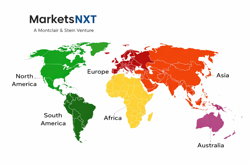
| Largest Market by Region | North America (approximately 52% — hyperscaler data centre concentration; NVIDIA/AMD HQ) |
| Fastest Growing Region | Asia Pacific (China domestic AI chip demand; Japan sovereign AI computing investment; South Korea HBM supply) |
| Segments Covered | Data Centre Training GPUs, Data Centre Inference Accelerators, Custom Hyperscaler AI Silicon (TPU, Trainium, Maia), Edge AI NPUs, Automotive and Robotics AI Chips |
| Competitive Intensity | Very High — NVIDIA dominant but challenged by AMD, Intel, custom silicon, and Chinese alternatives |
Regional Intelligence
North America holds approximately 52% of AI chip market revenue — concentrated in US hyperscaler data centres (Amazon, Microsoft, Google, Meta) that are the primary purchasers of NVIDIA data centre GPUs, AMD AI accelerators, and their own custom silicon. NVIDIA, AMD, and Intel are all headquartered in the US, concentrating the AI chip design ecosystem despite TSMC Taiwan manufacturing dependency. Export controls — NVIDIA's H100/H200 and AMD MI300 are restricted from sale to China under BIS Entity List and CCL restrictions — have created a bifurcated global market that has accelerated China's domestic AI chip development. Asia Pacific holds approximately 28% — China's Huawei Ascend 910B (competitive with NVIDIA A100 in some benchmarks) and Biren Technology's BR100 GPU represent the domestic AI chip capability developed in response to US export controls; South Korea's Samsung and SK Hynix supply HBM (High Bandwidth Memory) that is critical to AI GPU performance; Taiwan's TSMC manufactures essentially all leading-edge AI chips regardless of design nationality. Europe holds approximately 12%, with no European AI chip design company at commercial scale — a gap that EU's Chips Act is attempting to address through fab investment incentives.
Leading Market Participants
- NVIDIA Corporation (H100, H200, Blackwell B100/B200 GPUs)
- AMD (MI300X/MI300A AI accelerators)
- Google (TPU v5 — internal and cloud)
- Amazon Web Services (Trainium2, Inferentia2)
- Intel (Gaudi3 AI accelerator)
- Microsoft (Maia 100 custom AI chip)
- Meta (MTIA custom inference chip)
- Qualcomm (Cloud AI 100, edge NPU)
- Arm Holdings (AI IP licensing for NPU)
- Huawei (Ascend 910B — China market)
Frequently Asked Questions
Market Segmentation
- Data Centre AI Training GPUs (NVIDIA Hopper/Blackwell, AMD MI300)
- Custom Hyperscaler AI Silicon (Google TPU, Amazon Trainium, Microsoft Maia)
- Data Centre AI Inference Accelerators
- Others (Edge AI NPUs, Automotive AI SoC, Neuromorphic Chips, AI FPGA)
- Hyperscale Cloud Data Centres
- Enterprise AI Server and On-Premise Data Centre
- Consumer Electronics (Smartphone, PC, Tablet AI)
- Automotive (ADAS, Autonomous Driving AI)
- Industrial and Robotics AI
- Direct OEM and Hyperscaler Supply (NVIDIA CSP programme)
- Server OEM Integration (Dell, HPE, Supermicro)
- Cloud AI Compute As-a-Service (GPU-as-a-Service)
- Consumer Electronics OEM SoC Integration
- North America
- Europe
- Asia Pacific
- Latin America
- Middle East and Africa
Table of Contents
Research Framework and Methodological Approach
Information
Procurement
Information
Analysis
Market Formulation
& Validation
Overview of Our Research Process
MarketsNXT follows a structured, multi-stage research framework designed to ensure accuracy, reliability, and strategic relevance of every published study. Our methodology integrates globally accepted research standards with industry best practices in data collection, modeling, verification, and insight generation.
1. Data Acquisition Strategy
Robust data collection is the foundation of our analytical process. MarketsNXT employs a layered sourcing model.
- Company annual reports & SEC filings
- Industry association publications
- Technical journals & white papers
- Government databases (World Bank, OECD)
- Paid commercial databases
- KOL Interviews (CEOs, Marketing Heads)
- Surveys with industry participants
- Distributor & supplier discussions
- End-user feedback loops
- Questionnaires for gap analysis
Analytical Modeling and Insight Development
After collection, datasets are processed and interpreted using multiple analytical techniques to identify baseline market values, demand patterns, growth drivers, constraints, and opportunity clusters.
2. Market Estimation Techniques
MarketsNXT applies multiple estimation pathways to strengthen forecast accuracy.
Bottom-up Approach
Aggregating granular demand data from country level to derive global figures.
Top-down Approach
Breaking down the parent industry market to identify the target serviceable market.
Supply Chain Anchored Forecasting
MarketsNXT integrates value chain intelligence into its forecasting structure to ensure commercial realism and operational alignment.
Supply-Side Evaluation
Revenue and capacity estimates are developed through company financial reviews, product portfolio mapping, benchmarking of competitive positioning, and commercialization tracking.
3. Market Engineering & Validation
Market engineering involves the triangulation of data from multiple sources to minimize errors.
Extensive gathering of raw data.
Statistical regression & trend analysis.
Cross-verification with experts.
Publication of market study.
Client-Centric Research Delivery
MarketsNXT positions research delivery as a collaborative engagement rather than a static information transfer. Analysts work with clients to clarify objectives, interpret findings, and connect insights to strategic decisions.