Gallium Arsenide and III-V Semiconductor Materials Market Size, Share & Forecast 2026–2034
Report Highlights
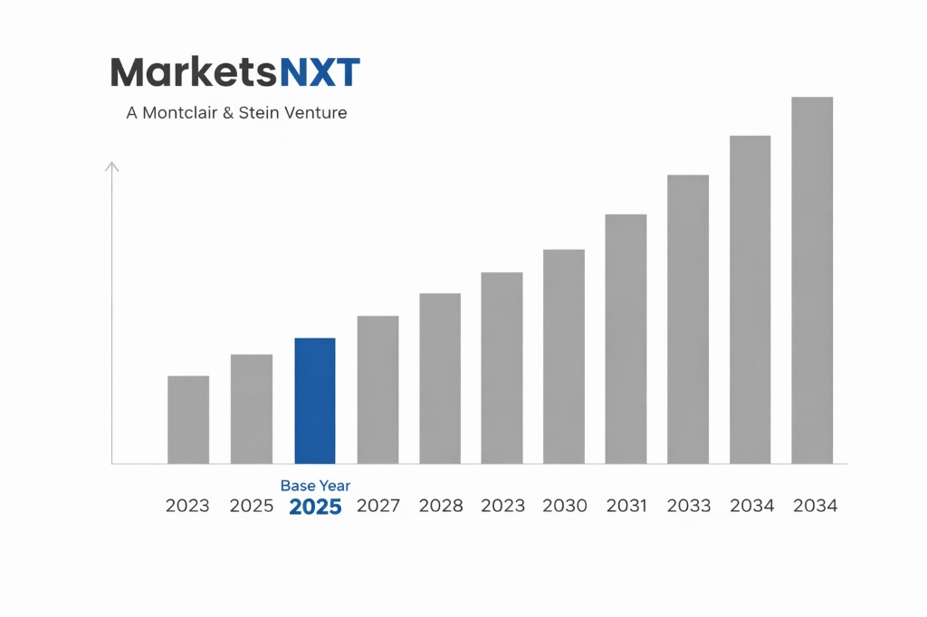
- ✓Market Size 2024: USD 1.4 billion
- ✓Market Size 2034: USD 11.5 billion
- ✓CAGR: 25.1%
- ✓Market Definition: Gallium arsenide (GaAs), indium phosphide (InP), gallium nitride (GaN), and related III-V compound semiconductor wafers, epitaxial structures, and devices for RF/microwave, photonic, power electronics, and solar cell applications, including substrate and epiwafer supply chains.
- ✓Leading Companies: Sumitomo Electric, Freiberger Compound Materials, AXT Inc., IQE, Qorvo
- ✓Base Year: 2025
- ✓Forecast Period: 2026–2034
How This Market Works
III-V semiconductor materials are compounds of elements from Groups III and V of the periodic table — gallium, indium, and aluminium combined with arsenic, phosphorus, and nitrogen — that provide electronic and photonic properties unachievable with silicon. The III-V materials market operates through a three-stage supply chain: upstream materials production (gallium and indium metal refined from zinc and aluminium smelter byproducts; arsenic, phosphorus, and nitrogen sourced from mining and industrial chemicals), substrate and wafer manufacturing (single-crystal III-V ingot growth by Liquid Encapsulated Czochralski or Vertical Gradient Freeze methods, followed by slicing, lapping, and polishing to produce epiready substrates), and epitaxial device structure growth (MOCVD or MBE deposition of functional device layers on substrates, producing high-frequency transistors, laser diodes, LEDs, and solar cell junctions).
The primary III-V compound families address distinct application windows determined by their bandgap and electron mobility properties. GaAs (gallium arsenide) dominates RF power amplifiers for smartphones, base stations, and satellite communications — its high electron mobility produces low-noise amplifiers and power amplifiers that silicon cannot replicate at microwave frequencies. GaN (gallium nitride) on silicon or silicon carbide substrates is the material of choice for high-power, high-frequency electronics in 5G base stations, military radar, and power conversion — its wide bandgap enables operation at higher voltages and temperatures than silicon. InP (indium phosphide) is the dominant material for coherent optical communications transmitters and receivers, datacentre interconnects, and next-generation photonic integrated circuits where silicon photonics cannot match InP's optical efficiency at 1,550 nm wavelength.
Who Controls This Market — And Who Is Threatening That Control
The III-V substrate market is controlled by a small number of specialised producers with no clear leader across all compound families. Sumitomo Electric Semiconductor Materials (Japan) is the largest global producer of GaAs substrates, holding approximately 25%–30% of global capacity. Freiberger Compound Materials (Germany) is a major GaAs and InP substrate supplier to European and US customers. AXT Inc. (US) produces GaAs, InP, and germanium substrates at facilities in China — a supply chain geography that creates geopolitical vulnerability given gallium export control dynamics. IQE (UK) is the world's largest independent epiwafer supplier — growing III-V epitaxial device structures on substrates for fabless semiconductor companies including Qorvo, Broadcom, and others that outsource epitaxy.
The most significant competitive threat is China's gallium supply control. China's August 2023 implementation of gallium and germanium export licensing requirements, tightened in December 2024, has created a formal mechanism for restricting gallium supply to Western III-V semiconductor manufacturers at a time when 5G infrastructure, defence electronics, and datacentre photonics demand are growing simultaneously. Western nations' gallium supply diversification response — recycling gallium from semiconductor manufacturing scrap, developing gallium recovery from fly ash and coal waste, and supporting new primary gallium production from bauxite refining outside China — is early-stage and cannot replace Chinese supply within a 5-year timeframe.
Industry Snapshot
The global III-V semiconductor market encompasses both the compound semiconductor materials market (substrates and epiwafers, approximately USD 1.6 billion in 2024) and the much larger market for III-V-based devices (RF chips, power electronics, laser diodes, photovoltaic cells, approximately USD 25 billion in 2024). The materials market is the foundational supply chain chokepoint — without substrates and epiwafers meeting the specifications for each device application, the device market cannot operate regardless of downstream demand. GaAs RF chips for smartphones represent the largest volume application, with approximately 4 billion GaAs power amplifier chips shipped annually for 4G/5G handset applications. GaN power electronics for data centre power conversion and EV inverters represent the fastest-growing application, growing at 40%+ annually from a base of approximately USD 1.2 billion in 2024 as GaN displaces silicon MOSFETs and IGBTs in high-efficiency power conversion applications.
The Forces Accelerating Demand Right Now
5G infrastructure rollout is driving simultaneous demand across multiple III-V material categories. 5G base stations require GaN power amplifiers (higher frequency operation than 4G), GaAs low-noise amplifiers for receive chains, and InP photonic components for the fronthaul optical connections between baseband units and remote radio heads. The density of 5G small cell deployments — estimated at 10–15× more base station units per square kilometre than 4G in dense urban coverage — multiplies the per-base-station III-V content across a much larger number of deployment units. Defence electronics demand for GaN and GaAs is growing at 20%+ annually, driven by hypersonic missile guidance systems, phased-array radar upgrades (LTAMDS, IBCS in the US; ASTER-30 upgrades in Europe), electronic warfare systems, and next-generation fighter aircraft active electronically scanned array (AESA) radar platforms that use thousands of GaN T/R modules per system. Space photovoltaics — multi-junction GaAs solar cells achieving 29%–32% conversion efficiency versus 20%–24% for silicon — are the standard power source for commercial and government satellites, and the LEO constellation buildout (Starlink, Kuiper, OneWeb) is driving unprecedented demand for space-grade GaAs solar cells.
What Is Holding This Market Back
Gallium supply concentration is the most acute structural risk in the market. China produces approximately 80% of global primary gallium from smelter byproduct streams, and the export licensing regime creates a discretionary supply restriction mechanism that is independent of commercial market conditions. Western III-V manufacturers cannot rapidly substitute Chinese gallium: recycling of gallium from semiconductor manufacturing scrap recovers approximately 50%–60% of input gallium but does not address net supply expansion; primary gallium production outside China from bauxite refining is technically feasible but economically marginal at current gallium prices (approximately USD 220–280/kg), requiring either higher prices or government subsidies to incentivise new capacity. The capital intensity and technical complexity of III-V substrate manufacturing — requiring ultra-high-purity starting materials, controlled crystal growth environments, and highly trained operators — creates long lead times (3–5 years for a new substrate facility) that cannot be accelerated by capital availability alone.
The Investment Case: Bull, Bear, and What Decides It
The bull case for III-V semiconductor investment is grounded in the irreplaceable performance of compound semiconductors in their target applications — there is no silicon-based substitute for GaN in 5G base station power amplifiers, no silicon alternative for InP in coherent optical transceivers at 400G–1.6T data rates, and no silicon solar cell competitive with multi-junction GaAs for space power applications. These application-specific monopolies mean demand is tied to 5G infrastructure growth, data centre bandwidth expansion, and space asset deployment rather than to semiconductor market cycles. The supply chain vulnerability created by China's gallium controls is simultaneously a risk and an investment opportunity — Western government investment in secure III-V supply chains (US DPA Title III programme, EU Critical Raw Materials Act) is creating subsidised capital for substrate manufacturing expansion outside China.
The bear case centres on the gradual erosion of III-V application windows by silicon-adjacent technologies. Silicon photonics (using silicon with germanium layers for optical modulation) is progressively capturing lower-performance data centre optical applications where InP once had monopoly position. GaN on silicon substrates, by reducing substrate cost compared to GaN on SiC, is expanding GaN's addressable market while simultaneously commoditising the substrate supply chain. The decisive variable is whether China's gallium export restrictions remain in place long enough to incentivise viable Western gallium supply alternatives — if controls are relaxed within 2–3 years, Western supply chain investment loses its economic justification.
Where the Next USD Billion Is Being Built
GaN power electronics for electric vehicle inverters is the highest-growth near-term III-V application. EV inverters converting DC battery power to AC motor drive traditionally use silicon IGBT switches; GaN-based inverters at the same power level operate at higher switching frequencies, enabling smaller passive components, and achieve 2%–3% higher system efficiency at a cost premium that is justified by the EV range improvement. Wolfspeed's GaN on SiC wafer capacity expansion at its Mohawk Valley fab (the world's largest SiC fab) is the most significant single capital investment in III-V power electronics infrastructure, supported by USD 750 million in CHIPS Act grants. InP photonic integrated circuits for datacentre co-packaged optics — integrating laser sources, modulators, and photodetectors on a single InP chip co-packaged with the AI switch ASIC — is an emerging USD 2–3 billion opportunity as AI datacentre bandwidth requirements make electrical I/O energy consumption unacceptable at scale.
Market at a Glance
| Parameter | Details |
|---|---|
| Market Size 2024 | USD 1.4 billion |
| Market Size 2034 | USD 11.5 billion |
| Growth Rate | 25.1% CAGR (2026–2034) |
| Most Critical Decision Factor | Technology maturity and regulatory readiness |
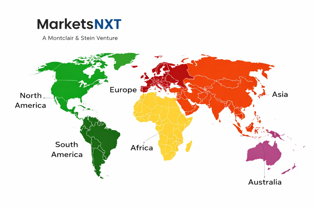
| Largest Region | Asia-Pacific |
| Competitive Structure | Fragmented — multiple platform and specialist players |
Regional Intelligence
Asia-Pacific dominates III-V semiconductor substrate and device production — Japan (Sumitomo Electric, MARUWA), Taiwan (WIN Semiconductors, AWSC — the leading GaAs foundries), and China (gallium supply, AXT substrate production) collectively control the majority of global III-V materials and wafer capacity. The Taiwan GaAs foundry ecosystem — WIN Semiconductors and AWSC supplying Qorvo, Broadcom, and other fabless RF chip companies — is the most commercially significant III-V manufacturing concentration, representing a supply chain concentration risk for Western RF chip companies analogous to logic semiconductor concentration at TSMC. North America's III-V investment is concentrated in defence and space applications (Coherent Corp., MACOM, Wolfspeed) with government-backed capacity expansion driven by CHIPS Act and DoD supply chain resilience programmes. Europe's III-V ecosystem is anchored by Freiberger Compound Materials (Germany) for substrates, IQE (UK) for epiwafers, and an academic-industrial research cluster in Germany and the Netherlands for next-generation III-V photonics.
Leading Market Participants
- Sumitomo Electric
- IQE is the world
- Wolfspeed
- Qorvo
- Broadcom
Long-Term Market Perspective
By 2034, III-V semiconductors will be more strategically critical than in 2024, not less — their role in 6G communications (TeraHertz frequency GaN/InP devices), next-generation photonic AI computing (InP photonic integrated circuits), and space solar power (high-efficiency multi-junction GaAs cells) ensures growing demand that silicon alternatives cannot address within the forecast period. The gallium supply chain will be partially diversified outside China through government-backed investment, but Chinese production will maintain its dominant share — the strategic risk will be managed through inventory stockpiling, recycling efficiency improvements, and diplomatic engagement rather than eliminated through supply chain reshoring. The III-V materials market's long-term structure will be defined by whether the compound semiconductor device market grows from its current USD 25 billion scale to USD 100+ billion by 2034 — a trajectory that requires both 5G and AI infrastructure growth continuing at current pace and GaN power electronics achieving mainstream automotive and data centre penetration on schedule.
Frequently Asked Questions
Market Segmentation
Table of Contents
Research Framework and Methodological Approach
Information
Procurement
Information
Analysis
Market Formulation
& Validation
Overview of Our Research Process
MarketsNXT follows a structured, multi-stage research framework designed to ensure accuracy, reliability, and strategic relevance of every published study. Our methodology integrates globally accepted research standards with industry best practices in data collection, modeling, verification, and insight generation.
1. Data Acquisition Strategy
Robust data collection is the foundation of our analytical process. MarketsNXT employs a layered sourcing model.
- Company annual reports & SEC filings
- Industry association publications
- Technical journals & white papers
- Government databases (World Bank, OECD)
- Paid commercial databases
- KOL Interviews (CEOs, Marketing Heads)
- Surveys with industry participants
- Distributor & supplier discussions
- End-user feedback loops
- Questionnaires for gap analysis
Analytical Modeling and Insight Development
After collection, datasets are processed and interpreted using multiple analytical techniques to identify baseline market values, demand patterns, growth drivers, constraints, and opportunity clusters.
2. Market Estimation Techniques
MarketsNXT applies multiple estimation pathways to strengthen forecast accuracy.
Bottom-up Approach
Aggregating granular demand data from country level to derive global figures.
Top-down Approach
Breaking down the parent industry market to identify the target serviceable market.
Supply Chain Anchored Forecasting
MarketsNXT integrates value chain intelligence into its forecasting structure to ensure commercial realism and operational alignment.
Supply-Side Evaluation
Revenue and capacity estimates are developed through company financial reviews, product portfolio mapping, benchmarking of competitive positioning, and commercialization tracking.
3. Market Engineering & Validation
Market engineering involves the triangulation of data from multiple sources to minimize errors.
Extensive gathering of raw data.
Statistical regression & trend analysis.
Cross-verification with experts.
Publication of market study.
Client-Centric Research Delivery
MarketsNXT positions research delivery as a collaborative engagement rather than a static information transfer. Analysts work with clients to clarify objectives, interpret findings, and connect insights to strategic decisions.