Semiconductor Packaging Substrates Market Size, Share & Forecast 2026–2034
Report Highlights
- ✓Market Size 2024: $16.8 billion
- ✓Market Size 2034: $31.2 billion
- ✓CAGR: 6.4%
- ✓Market Definition: Semiconductor packaging substrates are insulating materials that provide electrical connections between semiconductor dies and printed circuit boards, supporting mechanical mounting and thermal management. These substrates enable signal routing, power distribution, and heat dissipation in advanced semiconductor packages.
- ✓Leading Companies: ASE Group, Amkor Technology, JCET, Powertech Technology, ChipMOS Technologies
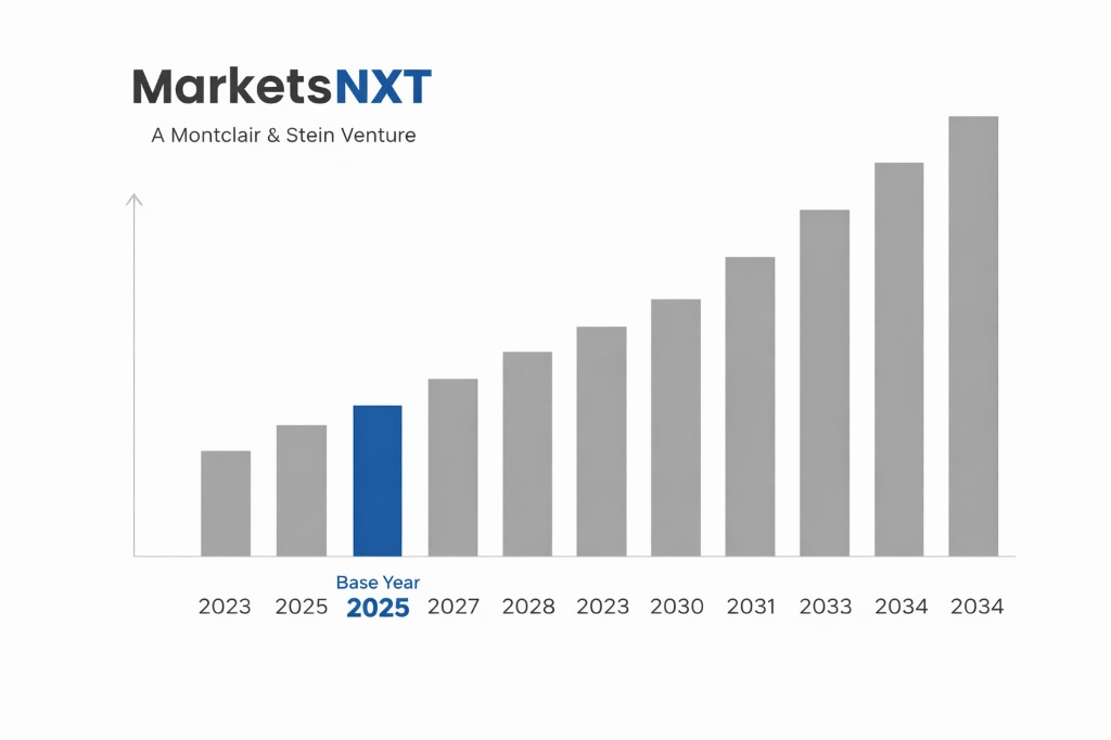
- ✓Base Year: 2025
- ✓Forecast Period: 2026–2034
Analyst Recommendation — Secure ABF Capacity: Semiconductor companies should lock long-term ABF substrate contracts before Q3 2026, as AI chip demand will exhaust available capacity and trigger 40% price increases through 2028.
Who Controls the Semiconductor Packaging Substrates - and Who Is Challenging That
ASE Group commands the largest share of semiconductor packaging substrate assembly with over 20% global market position, leveraging its integrated OSAT model that combines substrate manufacturing with assembly services. The Taiwan-based giant's competitive moat stems from its comprehensive customer relationships spanning Apple, Qualcomm, and MediaTek, plus vertically integrated capabilities from substrate fabrication through final package testing. Amkor Technology holds second position with 15% market share, differentiated by its advanced flip-chip substrate expertise and strategic partnerships with memory manufacturers including Micron and SK Hynix. JCET rounds out the top three with 12% share, gaining ground through aggressive pricing and rapid expansion in automotive semiconductor substrates where reliability requirements favor their established manufacturing processes.
Powertech Technology and ChipMOS Technologies are mounting serious challenges through specialized focus areas that bypass traditional competitive barriers. Powertech has captured significant smartphone processor substrate business by developing ultra-thin substrates that enable thinner device profiles, directly threatening ASE's mobile market dominance. ChipMOS targets the memory substrate segment with cost-optimized manufacturing that undercuts established players by 15-20%. The competitive order will shift if Powertech successfully scales its advanced packaging substrate technology to data center applications, or if Chinese players like TFME and Tongfu Microelectronics overcome technology transfer restrictions to compete in high-end substrates. Market leadership could fragment as AI chip packaging demands exceed current substrate manufacturing capacity, creating opportunities for smaller specialized players to capture premium segments.
Semiconductor Packaging Substrates Dynamics: How the Market Operates Today
The semiconductor packaging substrate market operates through a complex value chain where substrate manufacturers source raw materials from specialized chemical companies, fabricate multi-layer interconnect structures, and supply finished substrates to OSAT providers or integrated device manufacturers. Critical materials include ABF films from Ajinomoto, copper foils from Mitsui Mining, and glass fabrics from Nittobo, creating supply dependencies that influence pricing and availability. Transaction structures typically involve long-term supply agreements with quarterly volume commitments and price adjustments tied to raw material costs. Leading substrate manufacturers maintain dedicated production lines for specific customer requirements, particularly for advanced applications requiring precise impedance control and thermal management capabilities.
Current market maturity reflects a consolidation phase where economies of scale determine competitive positioning, as advanced substrate manufacturing requires capital investments exceeding $500 million per facility. Technology shifts toward heterogeneous integration and chiplet architectures are actively reshaping substrate design requirements, demanding embedded bridge interconnects and advanced thermal interface materials. Regulatory pressures around supply chain localization are forcing geographic redistribution of manufacturing capacity, with U.S. and European customers seeking substrate sources outside Asia. The industry faces immediate disruption from AI accelerator packaging demands that stress existing substrate technologies beyond current thermal and electrical performance limits, requiring entirely new material compositions and manufacturing processes that only a few leading players can develop.
Semiconductor Packaging Substrates Demand Drivers
AI chip proliferation drives unprecedented demand for advanced packaging substrates capable of handling extreme power densities and thermal loads that traditional substrates cannot manage. NVIDIA's H100 and upcoming Blackwell architecture GPUs require substrates with thermal conductivity exceeding 400 W/mK and power delivery networks supporting over 1000 amperes, specifications that only cutting-edge ABF substrates can meet. Data center accelerator deployments are projected to consume 40% of all advanced substrate production by 2027, creating supply shortages that force substrate manufacturers to prioritize high-value AI applications over traditional computing segments. This demand concentration enables substrate producers to command premium pricing for AI-optimized products while driving massive capacity expansion investments.
Automotive semiconductor integration creates a secondary demand surge as electric vehicles integrate multiple processing units requiring specialized automotive-grade substrates with extended temperature ranges and vibration resistance. Tesla's FSD computer and similar autonomous driving platforms demand substrates that maintain signal integrity across temperature cycles from -40°C to 150°C, requiring automotive-specific substrate formulations. 5G infrastructure deployment sustains demand for RF-optimized substrates with precise dielectric properties, particularly for base station power amplifiers and millimeter-wave applications. Mobile device manufacturers' push toward thinner form factors drives demand for ultra-thin substrates below 0.3mm thickness, requiring advanced manufacturing techniques that only established players can execute reliably, creating sustainable competitive advantages for technology leaders.
Restraints Limiting Semiconductor Packaging Substrates Growth
Raw material supply bottlenecks create the most significant growth constraint, with ABF film production concentrated among three suppliers led by Ajinomoto's 70% market share. Manufacturing capacity for ABF films requires 18-month lead times for expansion and faces technical barriers that prevent new entrants from achieving comparable quality standards. Copper foil availability fluctuates with industrial demand cycles, while specialized glass fabrics suitable for high-frequency applications face production limitations from Japanese suppliers including Asahi Kasei and Nittobo. These material constraints force substrate manufacturers to allocate production capacity based on raw material availability rather than customer demand, limiting growth potential during high-demand periods.
Technology complexity barriers prevent rapid capacity scaling as advanced substrate manufacturing requires specialized equipment from limited suppliers and highly trained engineering personnel with expertise in multi-layer interconnect design. Each new substrate generation demands 2-3 years of process development and qualification cycles with semiconductor customers, creating time lags between market demand emergence and production capacity availability. Geopolitical tensions restrict technology transfer and equipment access for Chinese manufacturers, while U.S. export controls limit advanced substrate technology sharing that historically enabled rapid industry expansion. Environmental regulations around chemical processing and waste management impose additional compliance costs that disproportionately impact smaller manufacturers, accelerating industry consolidation while limiting overall capacity growth.
Semiconductor Packaging Substrates Opportunities
Chiplet ecosystem development creates massive expansion opportunities for substrate manufacturers capable of developing heterogeneous integration platforms that connect diverse semiconductor functions within single packages. AMD's success with chiplet-based processors demonstrates market readiness for modular semiconductor architectures that require specialized substrate interconnects and embedded bridges. Intel's UCIe standard adoption across the industry will standardize chiplet interfaces, enabling substrate manufacturers to develop scalable product platforms serving multiple customers. Companies investing in advanced substrate technologies for chiplet integration can capture premium pricing and long-term customer relationships as traditional monolithic chip designs transition to modular architectures across computing, networking, and AI applications.
Automotive electrification presents untapped growth potential as electric vehicle adoption accelerates globally, requiring specialized power management substrates for inverters, charging systems, and battery management applications. Wide bandgap semiconductor adoption in automotive power electronics demands substrates optimized for silicon carbide and gallium nitride devices, creating niche markets with limited competition and premium pricing potential. Edge AI deployment across IoT devices opens opportunities for cost-optimized substrate solutions that balance performance requirements with volume manufacturing economics. Geographic expansion into emerging markets including India and Southeast Asia provides growth opportunities for substrate manufacturers seeking to establish local supply chains and capture regional semiconductor assembly business as these markets develop domestic capabilities.
Market at a Glance
| Metric | Value |
|---|---|
| Market Size 2024 | $16.8 billion |
| Market Size 2034 | $31.2 billion |
| Growth Rate (CAGR) | 6.4% |
| Most Critical Decision Factor | ABF material supply security |
| Largest Region | Asia Pacific |
| Competitive Structure | Consolidated with vertical integration |
Semiconductor Packaging Substrates by Region
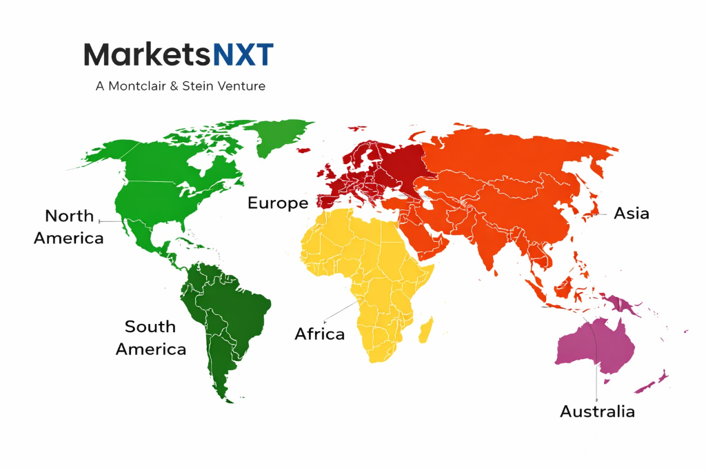
Asia Pacific dominates semiconductor packaging substrate production with 75% global market share, driven by Taiwan's OSAT industry concentration and China's massive electronics manufacturing base. Taiwan leads advanced substrate production through companies like ASE Group and Powertech Technology, benefiting from proximity to TSMC and other leading foundries that drive substrate technology requirements. South Korea contributes significantly through Samsung and SK Hynix's captive substrate capabilities for memory applications, while Japan maintains leadership in specialized substrate materials through Ajinomoto, Mitsui Mining, and other chemical suppliers. China represents the fastest-growing regional market with 8.2% CAGR through 2034, as domestic semiconductor companies including SMIC and Hua Hong expand packaging capabilities and government policies promote supply chain localization.
North America holds 15% market share with growth driven by AI chip demand from companies including NVIDIA, AMD, and Intel that require advanced substrate technologies for high-performance computing applications. The CHIPS Act incentivizes domestic substrate manufacturing capacity, with Intel planning substrate production facilities in Arizona and Ohio to support its foundry expansion plans. Europe maintains 8% market share focused on automotive and industrial applications, with Infineon and STMicroelectronics driving demand for specialized power semiconductor substrates. The region's strength in automotive electronics creates opportunities for substrate manufacturers targeting electric vehicle and autonomous driving applications that require specialized thermal and reliability characteristics unavailable from standard substrate products.
Leading Market Participants
- ASE Group
- Amkor Technology
- JCET
- Powertech Technology
- ChipMOS Technologies
- TFME
- Tongfu Microelectronics
- KYEC
- STATS ChipPAC
- Unisem
Competitive Outlook for Semiconductor Packaging Substrates
The semiconductor packaging substrate industry will experience significant consolidation over the next five years as technology complexity and capital requirements eliminate smaller players unable to invest in advanced manufacturing capabilities. AI chip packaging demands will create a bifurcated market where leading players including ASE Group, Amkor Technology, and JCET capture premium segments requiring cutting-edge thermal management and high-density interconnects, while cost-focused manufacturers serve traditional applications with limited growth potential. Strategic vertical integration will accelerate as OSAT companies acquire substrate specialists to secure supply chain control, similar to ASE Group's acquisition of substrate manufacturer Universal Scientific Industrial in 2021.
The most critical competitive development to monitor is raw material supply chain evolution, particularly Ajinomoto's potential expansion of ABF film production capacity and emergence of alternative suppliers that could disrupt current pricing dynamics. Chinese manufacturers face technology transfer restrictions that may permanently limit their access to advanced substrate technologies, potentially creating permanent competitive advantages for established Taiwan, South Korea, and Japan-based players. Chiplet architecture adoption will determine which substrate manufacturers successfully transition from traditional package-centric business models to platform-based solutions serving heterogeneous integration requirements, with winners capturing disproportionate market share as the industry restructures around modular semiconductor design paradigms.
Frequently Asked Questions
Market Segmentation
- Organic Substrates
- Ceramic Substrates
- Lead Frame Substrates
- Metal Core Substrates
- Flip Chip
- Wire Bonding
- Wafer Level Packaging
- Through Silicon Via
- System in Package
- Consumer Electronics
- Automotive
- Telecommunications
- Computing and Data Storage
- Industrial
- Healthcare
- Smartphones
- Tablets
- Laptops
- Servers
- Automotive ECUs
- IoT Devices
Table of Contents
Research Framework and Methodological Approach
Information
Procurement
Information
Analysis
Market Formulation
& Validation
Overview of Our Research Process
MarketsNXT follows a structured, multi-stage research framework designed to ensure accuracy, reliability, and strategic relevance of every published study. Our methodology integrates globally accepted research standards with industry best practices in data collection, modeling, verification, and insight generation.
1. Data Acquisition Strategy
Robust data collection is the foundation of our analytical process. MarketsNXT employs a layered sourcing model.
- Company annual reports & SEC filings
- Industry association publications
- Technical journals & white papers
- Government databases (World Bank, OECD)
- Paid commercial databases
- KOL Interviews (CEOs, Marketing Heads)
- Surveys with industry participants
- Distributor & supplier discussions
- End-user feedback loops
- Questionnaires for gap analysis
Analytical Modeling and Insight Development
After collection, datasets are processed and interpreted using multiple analytical techniques to identify baseline market values, demand patterns, growth drivers, constraints, and opportunity clusters.
2. Market Estimation Techniques
MarketsNXT applies multiple estimation pathways to strengthen forecast accuracy.
Bottom-up Approach
Aggregating granular demand data from country level to derive global figures.
Top-down Approach
Breaking down the parent industry market to identify the target serviceable market.
Supply Chain Anchored Forecasting
MarketsNXT integrates value chain intelligence into its forecasting structure to ensure commercial realism and operational alignment.
Supply-Side Evaluation
Revenue and capacity estimates are developed through company financial reviews, product portfolio mapping, benchmarking of competitive positioning, and commercialization tracking.
3. Market Engineering & Validation
Market engineering involves the triangulation of data from multiple sources to minimize errors.
Extensive gathering of raw data.
Statistical regression & trend analysis.
Cross-verification with experts.
Publication of market study.
Client-Centric Research Delivery
MarketsNXT positions research delivery as a collaborative engagement rather than a static information transfer. Analysts work with clients to clarify objectives, interpret findings, and connect insights to strategic decisions.